
User's Guide

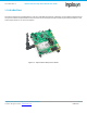
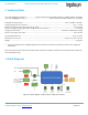
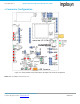
Table Of Contents
- 1. Introduction
- 2. Technical Data
- 3. Block Diagram
- 4. Connector Configuration
- 5. Test Points
- 6. LEDs
- 7. Schematic
- 8. Dimensions
- 9. Integration instructions for host product manufacturers according to KDB 996369 D03 OEM Manual v01
- 9.1. List of applicable FCC / ISED rules
- 9.2. Specific operational use conditions
- 9.3. Limited module procedures
- 9.4. Trace antenna designs
- 9.5. RF exposure considerations
- 9.6. Antennas
- 9.7. Label and compliance information
- 9.8. Information on test modes and additional testing requirements
- 9.9. Additional testing, Part 15 Subpart B disclaimer
- 9.10. Host Product Labelling Requirements
- 10. Disclaimer
- 11. References

NA-20-0386-0006-1.5 Inpixon Swarm Chirp V3 Dev Board User Guide
Inpixon_UG_Swarm_Chirp_V3_Dev_Board_1.5.docx 4
© Inpixon. All rights reserved. | www.inpixon.com FRM0008-A1
Contents
1. Introduction ............................................................................................................................................................................... 5
2. Technical Data ........................................................................................................................................................................... 6
3. Block Diagram ........................................................................................................................................................................... 6
4. Connector Configuration ......................................................................................................................................................... 7
4.1. Connector Description....................................................................................................................................................... 8
4.1.1. Connector J1 ................................................................................................................................................................. 8
4.1.2. Connector J2 ................................................................................................................................................................. 8
4.1.3. Connector X1 ................................................................................................................................................................ 9
4.1.4. Connector X2 ................................................................................................................................................................ 9
4.1.5. Connector X3 ................................................................................................................................................................ 9
4.1.6. Connector X4 .............................................................................................................................................................. 11
4.1.7. Connector X5 .............................................................................................................................................................. 11
4.1.8. Connector X6 .............................................................................................................................................................. 12
4.1.9. Connector X7 .............................................................................................................................................................. 12
4.1.10. Connector X8 ............................................................................................................................................................ 12
4.1.11. Connector X10 .......................................................................................................................................................... 12
4.1.12. Connector X11 .......................................................................................................................................................... 13
4.1.13. Connector X12 .......................................................................................................................................................... 13
4.1.14. Connector X13 .......................................................................................................................................................... 13
5. Test Points ............................................................................................................................................................................... 15
5.1. Test point TP10 Current Measurement ......................................................................................................................... 16
6. LEDs .......................................................................................................................................................................................... 18
7. Schematic ................................................................................................................................................................................. 19
8. Dimensions .............................................................................................................................................................................. 21
9. Integration instructions for host product manufacturers according to KDB 996369 D03 OEM Manual v01 ............ 22
9.1. List of applicable FCC / ISED rules .................................................................................................................................. 22
9.2. Specific operational use conditions ............................................................................................................................... 22
9.3. Limited module procedures ........................................................................................................................................... 22
9.4. Trace antenna designs .................................................................................................................................................... 22
9.5. RF exposure considerations ........................................................................................................................................... 22
9.6. Antennas ........................................................................................................................................................................... 22
9.7. Label and compliance information ................................................................................................................................ 23
9.8. Information on test modes and additional testing requirements ............................................................................ 24
9.9. Additional testing, Part 15 Subpart B disclaimer ......................................................................................................... 24
9.10. Host Product Labelling Requirements ........................................................................................................................ 25
9.10.1. FCC ............................................................................................................................................................................. 25
9.10.2. ISED ........................................................................................................................................................................... 25
10. Disclaimer .............................................................................................................................................................................. 26
10.1. FCC Disclaimer ................................................................................................................................................................ 26
10.2. ISED Statement ............................................................................................................................................................... 26
11. References ............................................................................................................................................................................. 27