
User's Guide
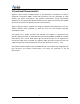
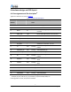
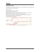
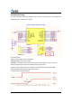
Table Of Contents

Allrightsreserved SuzhouPairlinkNetworkTechnologyLtd.
- 9 -
4.2.ReferenceDesign
The latest schematic and design examples, bill of material, and layout file are available from
originaldeveloper.Contactusfordetails.
Figure2:ModuleReferenceDesign
CircuitDescription
1:VBATsupplyvoltagevalueis2.70V‐3.60V.
2:PIN7(SPI_MOSI)reservedfortesting.
3:PIN9(RST_L)isModuleReset_Control(activeLow),Keepfloatingiftheuserisnotusing
4:ReserveJP1burninginterfaceifthePCBboardhasenoughspace.
5:TigerkinsupportGPIOssupermux,AllGPIOscanbedefinedasSPI/UART/I2C/PWM.
6:OnlyPI
N14(P0)andPIN15(P1)supportADCfunction.
7:TigerkinPoweronResetsequence.