
User's Guide
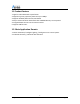
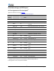
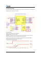
Table Of Contents

All rights reserved Suzhou Pairlink Network Technology Ltd.
- 8 -
4.2.Reference Design
The latest schematic and design examples, bill of material, and layout file are available from
original developer . Contact us for details.
Circuit Description
1:VBAT supply voltage value is 2.70V-3.60V.
2:PIN7(SPI_MOSI) reserved for testing.
3:PIN9(RST_L) is Module Reset_Control (active Low) ,Keep floating if the user is not using
4:Reserve JP1 burning interface if the PCB board has enough space.
5:Tigerkin support GPIOs supermux, All GPIOs can be defined as SPI /UART/I2C/PWM.
6:Only PIN14(P0) and PIN15(P1) support ADC function.
7:Tigerkin Power on Reset sequence.