
User's Guide


Buffalo-DS531-C User Guide
www.pairlink.com.cn
All rights reserved Suzhou Pairlink Network Technology Ltd.
- 6 -
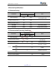
3.2.Reference Design
The latest schematic and design examples, bill of material, and layout file are available from
original developer . Contact us for details.
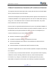
Figure 1: Module Reference Design
Circuit Description
1:VBAT supply voltage value is 1.80V-3.60V.
2:PIN10 (P0_9 / UART_RX), PIN11(P0.8 / UART_TX) is configured as the module's UART interface
by default.
3:PIN6(P0_0/RESET) multiplexing module RESET, software can be configured as RESET function,
internal pull-down by default.If need to configure the RESET function, must consult Pairlink for
recommendations.
4:The Buffalo-DS531-C is TTL level, and the uart port can communicate directly with the 3.3V
MCU.
5:Support GPIO super multiplexing function, WAKE_UP / UART / SPI / IIC / PWM / and other
functions can be arbitrarily configured on GPIO.
6:Reserve P1 burning interface if the PCB board has enough space.
7:The application diagram is shown below.