
User's Guide


Buffalo-DS531-C User Guide
www.pairlink.com.cn
All rights reserved Suzhou Pairlink Network Technology Ltd.
- 5 -
3.Hardware Design and PCB layout
3.1.Pin assignment and Pin description
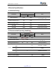
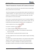
Buffalo-DS531-C Pin definition can refer to Figure 1.
Table 1: Module Pin Description
Pin Number
Pin Name
I/O
RESET STATE
Alternate Function Description
8
VBAT
P
Power Supply
1,15,16
GND
P
Connect to Ground
6
P0_0
DIO
I-PD
GPIO:P0_0
Reset
DI
I-PD
Reset signal (active high).
2
P0_6
DIO
I-PD
INPUT/OUTPUT with selectable pull
up/down resistor. General purpose
I/O port bit or alternate function
nodes. Contain state retention
mechanism during power down.
ADC2
AI
3
P0_2
DIO
I-PD
SWCLK
DIO
ADC1
AI
4
P0_10
DIO
I-PD
SWDIO
DIO
5
P0_11
DIO
I-PD
7
P0_1
DIO
I-PD
ADC0
AI
9
P0_3
DIO
I-PD
10
P0_9
DIO
I-PD
BLE_RX
DIO
11
P0_8
DIO
I-PD
BLE_TX
DIO
12
P0_5
DIO
I-PD
13
P0_4
AI
I-PD
14
P0_7
DIO
I-PD
ADC3
AI
Note: GPIO has integrated pull-up and pull-down resistors