
User`s manual


2-14
X6DH8-G2+/X6DHE-G2+ User's Manual
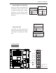
GLAN1
®
JLAN1
S
UPER X6DH8-G2+
GLAN2
DIMM 2B (Bank 2)
DIMM 2A (Bank 2)
DIMM 3B (Bank 3)
DIMM 3A (Bank 3)
DIMM 4B (Bank 4)
DIMM 4A (Bank 4)
DIMM 1A (Bank 1)
DIMM 1B (Bank 1)
Fan1
8-pin
PWR
PWR
SMBus
FP Control
SPK
PW LED
JP15
Fan2
JOH1
Fan8
Fan3
JL1
IPMI
IDE1
Floppy
COM2
BIOS
JWD
JPA1
SCSI CH A
Ultra 320
SCSI CH B
Fan4
JPA2
7902
CTRL
SATA0
SATA1
USB2/3
SMBUS
Speake
r
PCI-X #1 100 MHz ZCR
PCI-X #2 100 MHz
PCI-X
#3 133 MHz
WOR
Battery
JPL1
GLAN
CTLR
RAGE-
X
USB4
82546
GLAN
Enable
X4 PCI-Epx #4
X8 PCI-Epx #5
X8 PCI-Epx #6
Super
I/O
North
Bridge
JPG1
VGA
COM1
USB0/1
KB/
Mouse
Fan6
Fan5
ATX PWR
4-Pin
PWR
JPF
Parrallel
Port
24-Pin
Fan7
JP14
SCSI
JPA3
CPU 1
CPU 2
JBT1
ICH5R
SI/O
PXH
WOL
Ultra 320
IDE2
JP12
JP13
JLAN1
JLAN2
SEPC
South
Bridge
E7520
J27
DA1
DA2
LE1
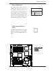
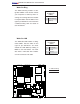
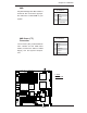
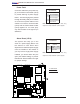
Universal Serial Bus
(USB0/1)
Two USB 2.0 ports (JPUSB1) are
located beside the PS/2 keyboard/
mouse ports. USB0 is the bottom
connector and USB1 is the top con-
nector. See the table on the right for
pin defi nitions.
Chassis Intrusion
A Chassis Intrusion header is located
at JL1. Attach the appropriate cable to
inform you of a chassis intrusion.
Universal Serial Bus
Pin Defi nitions (USB0/1)
USB0
Pin # Defi nition
USB1
Pin # Defi nition
1 +5V 1 +5V
2 PO- 2 PO-
3 PO+ 3 PO+
4 Ground 4 Ground
5N/A 5Key
Chassis Intrusion
Pin Defi nitions (JL1)
Pin# Defi nition
1 Intrusion Input
2 Ground
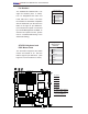
B
A
A. Chassis Intrusion
B. USB 0/1