
User Manual


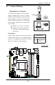


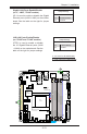


Table Of Contents
- Preface
- Chapter 1 Introduction
- Chapter 2 Installation
- 2-1 Standardized Warning Statements
- 2-2 Static-Sensitive Devices
- 2-3 Motherboard Installation
- 2-4 Memory Support
- 2-5 Connectors/IO Ports
- 2-6 Connecting Cables
- ATX PWR, DC PWR and HDD PWR Connectors (JPW1, PJ1, J6)
- Fan Headers (FAN1 ~ FAN4) (FAN4 is available on PCB 2.00 only)
- Chassis Intrusion
- System Management Bus Header
- DOM PWR Connector
- TPM Header/Port 80 Header
- Overheat LED Header
- Speaker
- Standby Power
- I-SGPIO1/I-SGPIO2
- NVMe I2C Header
- Power SMBus (I2C) Connector (available on PCB 2.00 only)
- System Management Bus Header
- GPIO Header
- ATX PWR, DC PWR and HDD PWR Connectors (JPW1, PJ1, J6)
- 2-7 Jumper Settings
- 2-8 Onboard Indicators
- 2-9 SATA Connections
- Chapter 3 Troubleshooting
- Chapter 4 BIOS
- Appendix A BIOS Error Beep Codes
- Appendix B Software Installation Instructions
- Appendix C UEFI BIOS Recovery Instructions
- Appendix D Dual Boot Block

2-26
X10SDV Mini-ITX Series Motherboard User’s Manual
JF1
JPI2C1
COM1
I-SATA0
JGPIO1
JSMB1
JPTG1
JBR1
JI2C1
JI2C2
JPG1
JPL1
JPME1
JPME2
JPUSB1
JWD1
DESIGNED IN USA
SRW2
SRW1
JUIDB1
J21
I-SGPIO2
I-SGPIO1
JL1
JOH1
JD1
PJ1
JSTBY1
JPW1
LED8
C
LED7
A
C
LED3
A
C
LEDM1
A
C
BT1
FAN4
FAN3
FAN2
FAN1
VGA
JTPM1
JSD1
I-SATA1
I-SATA4
I-SATA2
I-SATA3
I-SATA5
DIMMB2
DIMMA2
DIMMB1
DIMMA1
JIPMB1
JNVI2C1
X10SDV-F
REV: 2.00
LAN3/4
LAN1/2
PCI-E 3.0 X16
PWR
ON
RST
NIC2
OH
FF
X
NIC1
PWR
LED
HDD
LED
JF1:
USB 2/3
USB 0/1(3.0)
USB 4/5
SLOT7
JBT1
IPMI_LAN
J6
Intel
D-1500
BMC
AST2400
i350
GPIO Header
Pin Denitions
Pin# Denition Pin Denition
1 P3V3 2 GND
3 GP0 4 GP1
5 GP2 6 GP3
7 GP5 8 GP5
9 GP6 10 GP7
GPIO Header
The JGPIO1 header is located near the
SATA connectors on the motherboard.
The JGPIO header is a general purpose
I/O on a pin header. See the table on
the right for pin denitions. Refer to the
board layout below for the locations of
the headers.
A. GPIO Header
A
GPIO Register Address Table To Control JGPIO Pin Header
JGPIO1 PIN# SoC GPIO# USE Select IO Select Level
1 Power
2 Ground
3 17 IO 0x500 [17] IO 0x504 [17] IO 0x50C [17]
4 68 IO 0x540 [4] IO 0x544 [4] IO 0x548 [4]
5 01 IO 0x500 [1] IO 0x504 [1] IO 0x50C [1]
6 69 IO 0x540 [5] IO 0x544 [5] IO 0x548 [5]
7 06 IO 0x500 [6] IO x0504 [6] IO 0x50C [6]
8 70 IO 0x540 [6] IO 0x544 [6] IO 0x548 [6]
9 07 IO 0x500 [7] IO 0x504 [7] IO 0x50C [7]
10 71 IO 0x540 [7] IO 0x544 [7] IO 0x548 [7]
Note: Please refer to the Intel Xeon Processor D-1500 Product Family
Datasheet for more information.