
Datasheet


Datasheet 41
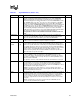
3.9 Processor Pinout Coordinates
Figure 10 and Figure 11 show the top and bottom view of the processor pin coordinates,
respectively. The coordinates are referred to throughout the document to identify processor pins.
Figure 10. Processor Pinout Coordinates, Top View
Vcc/Vss
ADDRESS
DATA
Vcc/Vss
CLOCKS
COMMON
CLOCK
COMMON
CLOCK
Async /
JTAG
Intel® Xeon™
Processor
Top View
= Signal
= Power
= Ground
= Reserved/No Connect
A
C
E
G
J
L
N
R
U
W
AA
AC
AE
B
D
F
H
K
M
P
T
V
Y
AB
AD
3 5 7 9 11 13 15 17 19 21 23 25 27 29 311
= GTLREF
A
C
E
G
J
L
N
R
U
W
AA
AC
AE
B
D
F
H
K
M
P
T
V
Y
AB
AD
2 4 6 8 10 12 14 16 18 20 22 24 26 28
30
(800 MHz)
= V
TT