
User`s manual


1-4
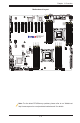
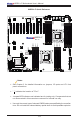
X9DRX+-F Motherboard User’s Manual
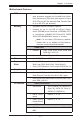
Notes:
•See Chapter 2 for detailed information on jumpers, I/O ports and JF1 front
panel connections.
•" " indicates the location of "Pin 1".
•Jumpers/LED Indicators not indicated are for testing only. Components that are
not documented in this manual are reserved for internal use only.
•Use only the correct type of onboard CMOS battery as specied by the manufac-
turer. Do not install the onboard battery upside down to avoid possible explosion.
X9DRX+-F Quick Reference
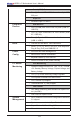
S-SATA0
S-SATA1
S-SATA2
S-SATA3
I-SATA0
FAN/PCH
SP1
JSD1
JPI2C1
JPW4
JITP2
BIOS
LED3
FAN8/CPU2
FAN7/CPU1
FAN6
FAN5
FAN1
FANA
FAN4
FANB
JVRM_I2C2
JVRM_I2C1
JPG1
JPL1
JPB1
JWD1
JPW1
J4
JPW3
JPW2
3-SPGPIO3
3-SPGPIO1
3-SPGPIO2
JIPMI1
JF1
JI2C1
JI2C2
JL1
JOH1
JD1
JSTBY1
JTPM1
JBAT1
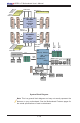
(IN X8)
KB/MOUSE
USB2/3
IPMI_LAN
TPM/PORT80
CPU2 Slot 7 PCI-E 3.0 x 8
CPU2 Slot 5 PCI-E 3.0 x 8
CPU1 Slot 3 PCI-E 3.0 x 8
CPU1 Slot 1 PCI-E 3.0 x 8
USB8/9
USB6/7
CPU1
CPU2
P2-DIMMG1
P2-DIMMH2
P2-DIMMH1
P2-DIMMG2
P2-DIMME2
P2-DIMME1
P2-DIMMF2
P2-DIMMF1
P1-DIMMD1
P1-DIMMC2
P1-DIMMC1
P1-DIMMD2
P1-DIMMA1
P1-DIMMA2
P1-DIMMB1
CPU1 Slot 2 PCI-E 3.0 x 8
CPU1 Slot 4 PCI-E 3.0 x 8
CPU2 Slot 6 PCI-E 3.0 x 8
CPU1 Slot 8 PCI-E 3.0 x 8
CPU2 Slot 9 PCI-E 3.0 x 8
CPU2 Slot 10 PCI-E 3.0 x 8
CPU2 Slot 11 PCI-E 2.0 x 4
P1-DIMMB2
COM2
UID
VGA
LAN2
LAN1
COM1
I-SATA2
I-SATA4
I-SATA1
I-SATA3
I
-
SATA 5
JPT1
USB4
USB5
JITP1
LED1
BMC CTRL
LAN
CTRL
FAN2
LED2
JBT1
CPU2
X9DRX+-F
Rev.
1.01
PCH
CPU1
USB0/1
CPLD
BMC Firmware
Clock Chip