
User`s manual

Chapter 2: Installation
2-33
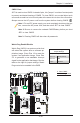
JPME1
JI2C1
VGA1
I-SATA1
I-SATA0
I-SATA5
I-SATA4
I-SATA3
I-SATA2
JIPMB1
JPME2
JPL1
JBR1
JWD1
JPG1
JPB1
JVRM_I2C1
JVRM_I2C2
JVR1
FAN5
FAN6
FAN8
FAN7
FAN1
FAN2
FAN3
FAN4
JF2
T-SGPIO1
T-SGPIO2
JUSB6
JSD1
JBT1
JBAT1
JTPM1
JF1
JPI2C1
JOH1
JI2C2
JL1
JSTBY1
JUIDB
J4
JD1
LED3
LEDM1
LED2
LAN2/4
LAN1/3
CPU1
CPU2
CPU2
CPU1
CPU2
CPU1
PWR I2C
UID
P2-DIMME1
P2-DIMMF2
P2-DIMMF1
P2-DIMMG2
P2-DIMMG1
P2-DIMMH2
P2-DIMMH1
P1-DIMMA2
P1-DIMMA1
P1-DIMMB2
P1-DIMMB1
P1-DIMMC1
P1-DIMMC2
P1-DIMMD1
P1-DIMMD2
USB4/5USB8/9
SLOT1 PCI-E 3.0 X8
SLOT2 PCI-E 3.0 X8
SLOT3 PCI-E 3.0 X8
SLOT4 PCI-E 3.0 X8
SLOT5 PCI-E 3.0 X8
USB6
TPM/PORT80
BUZZER
CMOS CLEAR
SLOT6 PCI-E 3.0 X8
COM2
USB2/3
COM1
USB0/1
SP1
CPU2
IPMI_LAN
CPU2
CPU2
Battery
BIOS
JPW1
JPW2
24-Pin Main PWR
8-Pin PWR
JPW4
P2-DIMME2
JPW3
8-Pin PWR
4-Pin PWR
L-SAS4~7
L-SAS0~3
LSI SAS CTRL
Intel
PCH
JPS1
LAN
CTRL
BMC
CPU1
X9DRD-7LN4F
Rev. 1.02
KB/Mouse
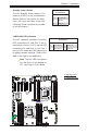
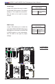
A
A. Standby PWR
B. LAN3/LAN4 LED
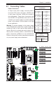
Standby Power Header
The +5V Standby Power header is lo-
cated at JSTBY1 on the motherboard.
See the table on the right for pin deni-
tions. (You must also have a card with
a Standby Power connector and a cable
to use this feature.)
Standby PWR
PinDenitions
Pin# Denition
1 +5V Standby
2 Ground
3 Wake-up
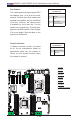
B
LAN3/LAN4 LED Indicators
The NIC (Network Interface Controller)
LED connections for LAN Port 3 are lo-
cated on pins 3 and 4 of JF2, and the LED
connections for LAN Port 4 is on Pins 1
and 2 of JF2. Attach NIC LED cables here
to display network activities. Refer to the
table on the right for pin denitions.
Note: The NIC LED connections
for LAN Ports 1/2 are located on
JF1. See Page 2-19 for details.
LAN Ports 3/4 LED Indicators (JF2)
PinDenitions
Pin# Denition Pin Denition
1 LAN4 Activity 2 LAN4 Link
3 LAN3 Activity 4 LAN3 Link