
User`s manual

Chapter 2: Installation
2-23
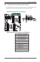
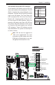
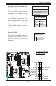
JPME1
JI2C1
VGA1
I-SATA1
I-SATA0
I-SATA5
I-SATA4
I-SATA3
I-SATA2
JIPMB1
JPME2
JPL1
JBR1
JWD1
JPG1
JPB1
JVRM_I2C1
JVRM_I2C2
JVR1
FAN5
FAN6
FAN8
FAN7
FAN1
FAN2
FAN3
FAN4
JF2
T-SGPIO1
T-SGPIO2
JUSB6
JSD1
JBT1
JBAT1
JTPM1
JF1
JPI2C1
JOH1
JI2C2
JL1
JSTBY1
JUIDB
J4
JD1
LED3
LEDM1
LED2
LAN2/4
LAN1/3
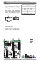
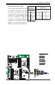
CPU1
CPU2
CPU2
CPU1
CPU2
CPU1
PWR I2C
UID
P2-DIMME1
P2-DIMMF2
P2-DIMMF1
P2-DIMMG2
P2-DIMMG1
P2-DIMMH2
P2-DIMMH1
P1-DIMMA2
P1-DIMMA1
P1-DIMMB2
P1-DIMMB1
P1-DIMMC1
P1-DIMMC2
P1-DIMMD1
P1-DIMMD2
USB4/5USB8/9
SLOT1 PCI-E 3.0 X8
SLOT2 PCI-E 3.0 X8
SLOT3 PCI-E 3.0 X8
SLOT4 PCI-E 3.0 X8
SLOT5 PCI-E 3.0 X8
USB6
TPM/PORT80
BUZZER
CMOS CLEAR
SLOT6 PCI-E 3.0 X8
COM2
USB2/3
COM1
USB0/1
SP1
CPU2
IPMI_LAN
CPU2
CPU2
Battery
BIOS
JPW1
JPW2
24-Pin Main PWR
8-Pin PWR
JPW4
P2-DIMME2
JPW3
8-Pin PWR
4-Pin PWR
L-SAS4~7
L-SAS0~3
LSI SAS CTRL
Intel
PCH
JPS1
LAN
CTRL
BMC
CPU1
X9DRD-7LN4F
Rev. 1.02
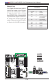
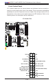
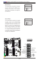
KB/Mouse
Power Button
Blue+ (OH/Fan Fail/
PWR FaiL/UID LED)
1
NIC1 Link LED
Reset Button
2
Power Fail LED
HDD LED
FP PWRLED
Reset
PWR
3.3 V
ID_UID_SW/3/3V Stby
Red+ (Blue LED Cathode)
Ground
Ground
1920
3.3V
X
Ground
NMI
X
NIC2 Link LED
NIC2 Activity LED
NIC1 Activity LED
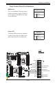
Power LED
The Power LED connection is located
on pins 15 and 16 of JF1. Refer to the
table on the right for pin denitions.
NMI Button
The non-maskable interrupt button
header is located on pins 19 and 20
of JF1. Refer to the table on the right
for pin denitions.
NMI Button
PinDenitions(JF1)
Pin# Denition
19 Control
20 Ground
Power LED
PinDenitions(JF1)
Pin# Denition
15 3.3V
16 PWR LED
FrontControlPanelPinDenitions
A. NMI
B. PWR LED
A
B