
User`s manual
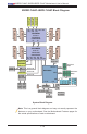

Chapter 1: Overview
1-5
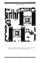
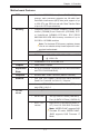
X9DRD-7LN4F-JBOD/-7LN4F Jumpers
Jumper
Description Default Setting
JBT1
Clear CMOS See Chapter 3
JI
2
C1/JI
2
C2
SMB to PCI-E Slots Off (Disabled)
JPB1 BMC Enabled Pins 1-2 (Enabled)
JPG1 VGA Enabled Pins 1-2 (Enabled)
JPL1 GLAN1/GLAN2 Enable Pins 1-2 (Enabled)
JPS1 SAS Enabled Pins 1-2 (Enabled)
JVRMI
2
C1/2 CPU1/2 VRM I
2
C Bus Pins 2-3 (Manufac-
ture Default)
JWD1 Watch Dog Timer Enable Pins 1-2 (Reset)
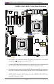
X9DRD-7LN4F-JBOD/-7LN4F Connectors
Connectors Description
COM1/COM2 Backplane COM Port1/Front Accessible COM2 Header
FAN1~8 CPU/System Fan Headers
JBAT1 Onboard Battery (See Chpt. 3 for Used Battery Disposal)
JD1 Speaker/Power LED Indicator
JF1 Front Panel Control Header
JF2 LAN3 (NIC3)/LAN4 (NIC4) LED Indicators
JIPMB1 4-pin External BMC I
2
C Header (for an IPMI Card)
JL1 Chassis Intrusion
JOH1 Overheat LED Indicator
JPI
2
C1 Power Supply SMBbus I
2
C Header
JPW1 24-Pin ATX Main Power Connector (Warning on Pg. 1-6.)
JPW2/3 12V 8-Pin Power Connectors (See Warning on Pg. 1-6.)
JPW4 12V 4-Pin Power Connectors (See Warning on Pg. 1-6.)
JSD1 SATA DOM (Device on Module) Power Connector
JSTBY1 +5V Standby Power Header
JTPM1 TPM (Trusted Platform Module)/Port 80
JUID UID (Unit Identication) Switch
LAN1/3, LAN2/4 Gigabit Ethernet Ports 1/2, 3/4
(IPMI) LAN IPMI_Dedicated LAN
(I)SATA1~6 Intel SATA Connectors 1~6 from the Intel PCH
(L)SAS0~3, 4~7 Serial_Link SCSI Attached 2.0 Connectors 0~3, 4~7 from
the LSI SAS 2308 Controller
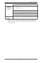
JP2 Manufacture (ME) Mode Pins 1-2 (Normal)
JPME1 ME Recovery Pins 1-2 (Normal)
JVRMI
2
C1/
JVRMI
2
C2
CPU1/CPU2 VRM SMbus Enable Pins 1-2 (Normal)
Note: PCI-E slots support Low-Prole MD2 form factor for devices/add-on
cards that are shorter than 167.64mm or 6.59" (in) in length only.