
User`s manual


2-22
X7DA8+/X7DAE+ User's Manual
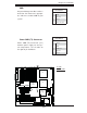
Compact Flash Card PWR
Connector
A Compact Flash Card Power Connector
is located at JWF1. For the Compact Flash
Card to work properly, you will need to
confi gure JCF1 properly and connect the
Compact Flash Card power cable to JWF1
fi rst. Refer to the board layout below for
the location.
Compact Flash Card PWR
Connector
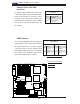
Jumper Defi nition
On Compact Flash
Power On
Off Compact Flash
Power Off
LAN1/2
®
S
UPER X7DA8+
Fan1
8-pin PWR
FP ControlSPK
PW LED
JOH1
Fan3
IDE1
Floppy
320 SCSI Channel A
Fan4
SATA3
SATA5
USB4/5
SMB
PCI-X 100 MHz ZCR (Green Slot)
PCI-X 133 MHz
JWD
Battery
GLAN
CTLR
JPG1
PCI-Exp x4
North Bridge
COM1
Fan6
Fan5
ATX PWR
4-Pin
PWR
J3P
24-Pin
SCSI CTRL
PXH
CPU1
CPU2
South Bridge
Fan7
JAR
J17
PSF
Fan2
Compact Flash
LE1
Fan8
JCF1
JWF1
JPA2
JPA3
JPA1
320 SCSI Channel B
SATA2
SATA4
SATA1
SATA0
JL1
PCI-X 133 MHz
JPL2
PCI-33MHz
FP Audio
PCI-Exp x16
SIM LP IPMI
DIMM 1A (Bank 1)
DIMM 1B (Bank 1)
DIMM 2A (Bank 2)
DIMM 2B (Bank 2)
DIMM 3A (Bank 3)
DIMM 3B (Bank 3)
DIMM 4A (Bank 4)
DIMM 4B (Bank 4)
JWOL
JWOR
KB/
Mouse
USB 0/
1/2/3
JI
2
C2
JI
2
C3
JI
2
C4
5000X
BIOS
DA1
DA2
CPU
Fan 1
CD1
JPL1
JI
2
C1
CPU
Fan2
HD
Audio
SGPIO1
SGPIO2
Parrallel
Port
Audio
CTRL
S I/O
J8
Clear
CMOS
ESB
Cha.
Intru.
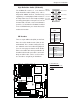
A. Compact Flash PWR
B. SGPIO 1
C. SGPIO 2
A
SGPIO Headers
There are two SGPIO (Serial General Purpose
Input/Output) headers (J29, J30) located on
the motherboard. These headers support
serial link interfaces for the onboard serial
link (SATA or SAS) connectors. See the table
on the right for pin defi nitions. Refer to the
board layout below for the location.
Note: NC= No Connections
B
C
SGPIO
Pin Defi nitions
Pin# Defi nition Pin Defi nition
1 *NC 2 *NC
3 Ground 4 DATA Out
5 Load 6 Ground
7 Clock 8 *NC