PDSML-LN1+ PDSML-LN2+ PDSML-E+ USER’S MANUAL Revision 1.
The information in this User’s Manual has been carefully reviewed and is believed to be accurate. The vendor assumes no responsibility for any inaccuracies that may be contained in this document, makes no commitment to update or to keep current the information in this manual, or to notify any person or organization of the updates. Please Note: For the most up-to-date version of this manual, please see our web site at www.supermicro.com. Super Micro Computer, Inc.
Preface Preface About This Manual This manual is written for system integrators, PC technicians and knowledgeable PC users. It provides information for the installation and use of the PDSML-LN1+/PDSML-LN2+/PDSML-E+ motherboard. It supports single Intel® Xeon® 3200/3000, Core™ 2 Duo Series, Pentium® D (Dual-Core), Pentium 4, and Celeron® D LGA (Land Grid Array) 775 Processors at system bus speeds of 1066/800/533 MHz.
PDSML-LN1+/PDSML-LN2+/PDSML-E+ User’s Manual Table of Contents Preface About This Manual ...................................................................................................... iii Manual Organization .................................................................................................... iii Conventions Used in the Manual .................................................................................. iii Chapter 1: Introduction 1-1 Overview .................................
Table of Contents Reset Button............................................................................................ 2-12 Power Button ........................................................................................... 2-12 2-6 Connecting Cables ....................................................................................... 2-13 ATX Power Connector .......................................................................... 2-13 Processor Power Connector ................................
PDSML-LN1+/PDSML-LN2+/PDSML-E+ User’s Manual Memory Errors........................................................................................... 3-2 Losing the System’s Setup Configuration ................................................ 3-2 3-2 Technical Support Procedures ........................................................................ 3-2 3-3 Frequently Asked Questions ...........................................................................
Chapter 1: Introduction Chapter 1 Introduction 1-1 Overview Checklist Congratulations on purchasing your computer motherboard from an acknowledged leader in the industry. Supermicro motherboards are designed with the utmost attention to detail to provide you with the highest standards in quality and performance. Please check that the following items have all been included with your motherboard. If anything listed here is damaged or missing, contact your retailer.
PDSML-LN1+/PDSML-LN2+/PDSML-E+ User’s Manual Contacting Super Micro Headquarters Address: Tel: Fax: Email: Web Site: Super Micro Computer, Inc. 980 Rock Ave. San Jose, CA 95131 U.S.A. +1 (408) 503-8000 +1 (408) 503-8008 marketing@supermicro.com (General Information) support@supermicro.com (Technical Support) www.supermicro.com Europe Address: Tel: Fax: Email: Super Micro Computer B.V.
Chapter 1: Introduction PDSML-LN1+/PDSML-LN2+/PDSML-E+ Image An Important Note to the User • All images and layouts shown in this manual were based upon the latest PCB Revision available at the time of publishing of this manual. The motherboard you've received may or may not look exactly the same as the graphics shown in this manual. • Please see Note 5 on Page 1-4.
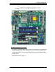
PDSML-LN1+/PDSML-LN2+/PDSML-E+ User’s Manual 24-Pin ATX PWR Fan6 KB/MS J28 USB 1/2 J15 PWR SMB PWRFault Fan1 JPL1 JPL2 LGA 775 CPU Intel 3000 OR Intel 3010 PDSML-E+ Only North Bridge ® SUPER JLAN1 JLAN2 PDSML-LN1+/LN2+/E+ DIMM 1A DIMM 1 DIMM 2A DIMM 2 Fan2 FP CTRL JG1 Fan3 JPF (*LN2+) DIMM 1B DIMM 2B IPMI COM2 PCI-E x4 J10 SPKR J 9 BIOS PCI-33 MHz Floppy J27 PCI1 JL1 ICH7R South Bridge USB3/4 USB5/6 J46 J45 JBT1 SATA1 SATA3 JS2 JS4 SATA0 SATA2 JS1 JS3 JLED Slot4 S I/O
Chapter 1: Introduction PDSML-LN1+/PDSML-LN2+/PDSML-E+ Quick Reference Jumpers Description Default Setting JBT1 CMOS Clear See Section 2-7 JI2 2 C1/JI C2 2 I C Bus to PCI Slots 1/2 Open (Disabled) JPF Power Force-On Open (Disabled) JPG1 VGA Enable Pins 1-2 (Enabled) JPL1/JPL2 (Note) Giga-bit LAN 1/2 Enable Pins 1-2 (Enabled) Connectors Description 24-PIn ATX (JPW1) ATX 24-pin Power Connector 8-Pin PWR (JPW2) 12V 8-pin PWR Connector Alarm Reset (JPR1) Redundant Power Alarm Reset
PDSML-LN1+/PDSML-LN2+/PDSML-E+ User’s Manual Motherboard Features Processor • Single Intel Xeon 3200/3000/Core 2 Duo Series//Pentium D dual-core/Pentium 4/Celeron D processors at system bus speeds of 1066/800/533 MHz. • Hyper-Threading (HT), EM64T, Enhanced Intel SpeedStep (EIST) supported The EM64T Feature is supported when: • 64-bit OS (Windows XP Professional x64 Ed, Server 2003x64 Ed.) and • 64-bit drivers for all MB components, devices and add-on cards are installed on the motherboard.
Chapter 1: Introduction ACPI Features • Slow blinking LED for suspend state indicator • BIOS support for USB keyboard/Mouse • Main switch override mechanism • External modem ring-on Onboard I/O • One ATA/100 EIDE Channel • Intel ICH7R SATA Controller, 4 connectors for 4 devices with support of RAID 0, 1, 5 and 10 (Note) • One floppy port interface (up to 2.
PDSML-LN1+/PDSML-LN2+/PDSML-E+ User’s Manual VRM V11 RDDA LRTC ATAD LRTC ATAD LGA775_PROCESSOR RDDA VRM 11 CK410 CLK FSB: 1066/800/533MHz DDR2 CH_A1-2 CH_B1-2 DDR2_667/533/400 Intel 3000 or Intel 3010 IMD 4 x SATA PORTS PCI-e x8 SLOT PCIE_x4 PCI-e x8 SLOT PCIE_x1 Gb_LAN PCIE_x1 Gb_LAN (PDSML-E+ Only) MCH PRI_IDE CF_HEADER PCIE_x8 UDMA/100 ICH-7R S-ATA/300 PCI_32_BUS Z7 PCI_32_BUS USB XGI_VGA LPC USB 2.0/1.1 2x PCI_32 SLOT PORTS 1~6 W83627HG LPC I/O KB. MS. FDD.
Chapter 1: Introduction 1-2 Chipset Overview The Intel 3000/3010 chipset is comprised of two primary components: the Memory Controller Hub (MCH) and the I/O Controller Hub (ICH7R). With the capabilities provided by the Intel 3000/3010 chipset, the PDSML-LN1+/PDSML-LN2+/PDSML-E+ provides the performance and feature-set required for cost-effective UP servers.
PDSML-LN1+/PDSML-LN2+/PDSML-E+ User’s Manual 1-3 Special Features Recovery from AC Power Loss BIOS provides a setting for you to determine how the system will respond when AC power is lost and then restored to the system. You can choose for the system to remain powered off (in which case you must hit the power switch to turn it back on) or for it to automatically return to a power- on state. See the Power Lost Control setting in the Advanced BIOS Setup section to change this setting.
Chapter 1: Introduction CPU Overheat LED and Control This feature is available when the user enables the CPU overheat warning function in the BIOS. This allows the user to define an overheat temperature. When this temperature exceeds the predefined temperature threshold, both overheat fan and the warning LED will be activated. System Resource Alert This feature is available when used with Supero Doctor III in the Windows OS environment or used with Supero Doctor II in Linux.
PDSML-LN1+/PDSML-LN2+/PDSML-E+ User’s Manual supply provides power to keep the required circuitry in the system alive. In case the system malfunctions and you want to turn off the power, just press and hold the power button for 4 seconds. This option can be set in the Power section of the BIOS Setup routine. External Modem Ring-On Wake-up events can be triggered by a device such as the external modem ringing when the system is in the Standby or Off state.
Chapter 1: Introduction 1-7 Super I/O The disk drive adapter functions of the Super I/O chip include a floppy disk drive controller that is compatible with industry standard 82077/765, a data separator, write pre-compensation circuitry, decode logic, data rate selection, a clock generator, drive interface control logic and interrupt and DMA logic. The wide range of functions integrated onto the Super I/O greatly reduces the number of components required for interfacing with floppy disk drives.
PDSML-LN1+/PDSML-LN2+/PDSML-E+ User’s Manual For more information on IPMI configuration, please refer to the AOC-SIM1U/SIM1U+ and AOC-SIMLC User’s Guide posted on our website at http://www.supermicro.com/ products/accessories/addon/SIM.cfm.
Chapter 2: Installation Chapter 2 Installation 2-1 Electro-Static Sensitive Devices Electro-Static Discharge (ESD) can damage electronic components. To ! prevent damage to your system board, it is important to handle it very carefully. The following measures are generally sufficient to protect your equipment from ESD. Precautions • Use a grounded wrist strap designed to prevent electro-static build up.
PDSML-LN1+/PDSML-LN2+/PDSML-E+ User's Manual 2-2 Processor, Heatsink and Fan Installation When handling the processor package, avoid placing ! direct pressure on the label area of the fan. Notes: 1. Always connect the power cord last and always remove it before adding, removing or changing any components. Make sure that you install the processor into the CPU socket before you install the CPU heatsink. 2. Intel's boxed processor package contains the CPU fan and heatsink assembly.
Chapter 2: Installation North Key 3. Locate Pin 1 on the CPU socket. Note: Pin 1 is the corner marked with a triangle. Please note that the North Key and the South Key are located vertically in the CPU housing. 4. Position the motherboard in such a way Pin 1 that Pin 1 of the CPU socket is located at the left bottom of the CPU housing. South Key North Center Edge 5. Use your thumb and your index finger to hold the CPU at the North Center Edge and the South Center Edge of the CPU. 6.
PDSML-LN1+/PDSML-LN2+/PDSML-E+ User's Manual Installation of the Heatsink 1. Locate the CPU Fan on the motherboard. (Refer to the layout on the right for the CPU Fan location.) 2. Position the heatsink so that the heatsink fan wires are closest to the SUPER ® PDSML-LN1+/LN2+/E+ CPU fan and are not interfered with other components. 3. Inspect the CPU Fan wires to make sure that the wires are routed through the bottom of the heatsink. 4.
Chapter 2: Installation 8. Repeat Step 6 to insert all four heatsink fasteners into the mounting holes. 9. Once all four fasteners are securely inserted into the mounting holes and the heatsink is properly installed on the motherboard, connect the heatsink fan wires to the CPU Fan connector. Heatsink Removal 1. Unplug the power cord from the power supply. 2. Disconnect the heatsink fan wires from the CPU fan header. 3.
PDSML-LN1+/PDSML-LN2+/PDSML-E+ User's Manual 2-4 Installing DDR2 Memory Memory Module Installation Exercise extreme care when installing or removing memory modules to prevent any possible damage. 1. Insert each DDR2 memory module vertically into its slot. Pay attention to the notch along the bottom of the module to prevent inserting the module incorrectly. (See support information below.) 2. Gently press down on the memory module until it snaps into place.
Chapter 2: Installation Possible System Memory Allocation & Availability System Device Size Physical Memory Remaining (-Available) (3 GB Total System Memory) Physical Memory Remaining (-Available) (4 GB Total System Memory) Firmware Hub flash memory (System BIOS) 1 MB 3.00 3.99 Local APIC 4 KB 3.00 3.99 Area Reserved for the chipset 2 MB 3.00 3.99 I/O APIC (4 Kbytes) 4 KB 3.00 3.99 PCI Enumeration Area 1 256 MB 3.00 3.76 PCI Express (256 MB) 256 MB 3.00 3.
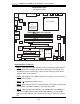
PDSML-LN1+/PDSML-LN2+/PDSML-E+ User's Manual 2-5 Control Panel Connectors/IO Ports The I/O ports are color coded in conformance with the PC 99 specification. See below for the colors and locations of the various I/O ports. A. Back Panel Connectors/IO Ports SUPER ® 2 4 1 3 PDSML-LN1+/LN2+/E+ 5 6 7 8 Back Panel I/O Port Locations and Definitions Back Panel Connectors 1. Keyboard (Purple) 5. COM Port 1 (Turquoise) 2. PS/2 Mouse (Green) 6. VGA Port (Blue) 3. Back Panel USB Port 1 7.
Chapter 2: Installation C. Front Control Panel Pin Definitions NMI Button NMI Button Pin Definitions (JF1) The non-maskable interrupt button Pin# Definition header is located on pins 19 and 20 19 Control 20 Ground of JF1. Refer to the table on the right for pin definitions. Power LED Power LED Pin Definitions (JF1) The Power LED connection is located Pin# Definition on pins 15 and 16 of JF1. Refer to 15 +5V the table on the right for pin defini- 16 Ground tions.
PDSML-LN1+/PDSML-LN2+/PDSML-E+ User's Manual HDD LED HDD LED Pin Definitions (JF1) The HDD LED connection is located on pins 13 and 14 of JF1. Attach the hard drive LED cable here to display Pin# Definition 13 +5V 14 HD Active disk activity (for any hard drives on the system, including Serial ATA and IDE if available). See the table on the right for pin definitions.
Chapter 2: Installation Overheat/FanFail LED OH/Fan Fail Indicator Status Connect an LED cable to the OH/Fan Fail connection on pins 7 and 8 of JF1 State to provide advanced warning of chas- Off sis overheating or system fan failure. Refer to the table on the right for pin definitions.
PDSML-LN1+/PDSML-LN2+/PDSML-E+ User's Manual Reset Button Reset Button Pin Definitions (JF1) The Reset Button connection is located on pins 3 and 4 of JF1. Attach Pin# Definition it to the hardware reset switch on the 3 Reset computer case. Refer to the table on the right for pin definitions. 4 Ground Power Button The Power Button connection is Power Button Pin Definitions (JF1) located on pins 1 and 2 of JF1. Momentarily contacting both pins will Pin# Definition power on/off the system.
Chapter 2: Installation 2-6 Connectors and Headers ATX Power 24-pin Connector Pin Definitions Pin# Definition 13 +3.3V 1 +3.3V The main power supply connec- 14 -12V 2 +3.3V tor (JPW1) on the PDSML-LN1+/ 15 COM 3 COM PDSML-LN2+/PDSML-E+ meets the 16 PS_ON 4 +5V Server System Infrastructure (SSI) 17 COM 5 COM specification. You can only use a 18 COM 6 +5V 24-pin power supply cable on the 19 COM 7 COM motherboard.
PDSML-LN1+/PDSML-LN2+/PDSML-E+ User's Manual Serial Ports Serial Port Pin Definitions (COM1/COM2) Two serial headers: COM1 (J31), Pin # COM2 are included on the motherboard. COM1 (J31) is a port located next to VGA port. See the table on the right for pin definitions. Definition Pin # Definition 1 CD 6 DSR 2 RD 7 RTS 3 TD 8 CTS 4 DTR 9 RI 5 Ground 10 NC Note: Pin 10 is included on the header but not on the port. NC indicates no connection.
Chapter 2: Installation Universal Serial Bus (USB) There are two Universal Serial Bus Universal Serial Bus Pin Definitions ports (BP USB 1/2) (J15) located on the I/O back panel and additional four Back Panel USB Pin # Definition USB ports located at J46 (FP USB 1 +5V 1 +5V 3/4) and J45 (FP USB 5/6) on the 2 PO- 2 PO- motherboard. These ports (FP USB3 3 PO+ 3 PO+ 4 Ground 4 Ground 5 N/A 5 Key /4, FPUSB 5/6) can be used to provide front side chassis access.
PDSML-LN1+/PDSML-LN2+/PDSML-E+ User's Manual ATX PS/2 Keyboard and PS/2 Mouse Ports PS/2 Keyboard and Mouse Port Pin Definitions The ATX PS/2 keyboard and PS/2 Pin# Definition mouse are located next to the Back 1 Data Panel USB ports on the motherboard. 2 NC See the table at right for pin defini- 3 Ground tions. (Note: NC=No connection.
Chapter 2: Installation Fan Headers Fan Header Pin Definitions (Fan1-5) The PDSML-LN1+/PDSML-LN2+/ PDSML-E+ has six fan connections (Fan1 to Fan6). Fan6 is designated as the CPU Cooling Fan. Note: all fans are 4-pin fans. Pin# Definition 1 Ground (Black) However, Pins 1-3 of the fan headers are 2 +12V (Red) backward compatible with the traditional 3 Tachometer 3-pin fans. See the table on the right for 4 PWM_Control pin definitions.
PDSML-LN1+/PDSML-LN2+/PDSML-E+ User's Manual Wake-On-Ring Wake-On-Ring Pin Definitions (JWOR) The Wake-On-Ring header is located at JWOR. This function allows an incoming call to the modem to "wake Pin# Definition up" your system when in the suspend 1 Ground (Black) state. See the table on the right for 2 Wake-up pin definitions. You must have a Wake-On-Ring card and cable to use this feature. Wake-On-LAN Wake-On-LAN Pin Definitions (JWOL) The Wake-On-LAN header is located at JWOL.
Chapter 2: Installation VGA Connector A VGA connector (JG1) is located next to the COM1 port on the IO backplane. Refer to the board layout below for the location. Power LED PWR LED Pin Definitions The Power LED connector is desigPin# Definition 1 +5V to indicate that power has been sup- 2 Key plied to the system. See the table on 3 Ground nated JLED. This connection is used for 3-pin LED applications. It is used the right for pin definitions.
PDSML-LN1+/PDSML-LN2+/PDSML-E+ User's Manual Power Fault PWR Fault Pin Definitions Connect a cable from your power supply to the Power Fault header (PW3) to provide warning of power supply failure. This warning signal is passed through the PWR_LED pin to indicate of a power failure on the chassis. See the table on the right for pin Pin# Definition 1 Pin 1 Fail Signal 2 Pin 2 Fail Signal 3 Pin 3 Fail Signal 4 Pin 4 Fail Signal Note: This feature is only available when using definitions.
Chapter 2: Installation Redundant PWR Alarm Reset Connector Redundant PWR Supply Alarm Reset Jumper Definition A Redundant Power Supply Fail Alarm Reset is located at JPR1. Refer to the board layout below for the location. On Enabled Off Disabled 24-Pin ATX PWR Fan6 KB/MS PWR SMB PWR Fault CPU Fan JPR1 A A.
PDSML-LN1+/PDSML-LN2+/PDSML-E+ User's Manual 2-7 Jumper Settings Explanation of Jumpers To modify the operation of the motherboard, jumpers can be used to choose between optional settings. Jumpers create shorts between two pins to change the function of the connector. Pin 1 is identified with a square solder pad on the printed circuit board. See the motherboard layout pages for jumper locations. Note: On two pin jumpers, "Closed" means the jumper is on and "Open" means the jumper is off the pins.
Chapter 2: Installation CMOS Clear JBT1 is used to clear CMOS. Instead of pins, this "jumper" consists of contact pads to prevent the accidental clearing of CMOS. To clear CMOS, use a metal object such as a small screwdriver to touch both pads at the same time to short the connection. Always remove the AC power cord from the system before clearing CMOS. Note: For an ATX power supply, you must completely shut down the system, remove the AC power cord and then short JBT1 to clear CMOS.
PDSML-LN1+/PDSML-LN2+/PDSML-E+ User's Manual Power Force On Enable/ Disable Power Force On Enable/Disable Jumper Settings (JPF) Jumper JPF allows you to enable or Jumper Setting disable the Power Force On function. If enabled, the power will always stay on automatically. If this function is disabled Definition Open Normal Closed Force On (the normal setting), the user needs to press the power button to power on the system.
Chapter 2: Installation 2-8 Onboard LED Indicators Activity Link GLAN LEDs (*Rear View: When facing the There are two GLAN ports on the PDSML-LN2+/PDSML-E+ and one rear side of the system) GLAN Activity LED Indicator GLAN port on the PDSML-LN1+. Each Gigabit Ethernet LAN port has two LED Color Definition LEDs.
PDSML-LN1+/PDSML-LN2+/PDSML-E+ User's Manual 2-9 Floppy, Hard Disk Drive and IPMI 2.0 Connections Note the following when connecting the floppy and hard disk drive cables: • The floppy disk drive cable has seven twisted wires. • A red mark on a wire typically designates the location of pin 1. • A single floppy disk drive ribbon cable has two connectors to provide for two floppy disk drives.
Chapter 2: Installation IDE Drive Connectors Pin Definitions (IDE) IDE Connector There is one IDE Connector (J3) on the motherboard. See the table on the right for pin definitions. IPMI 2.0 Slot (For PDSML-LN2+ and PDSML-E+ only) There is an IPMI 2.
PDSML-LN1+/PDSML-LN2+/PDSML-E+ User's Manual Notes 2-28
Chapter 3: Troubleshooting Chapter 3 Troubleshooting 3-1 Troubleshooting Procedures Use the following procedures to troubleshoot your system. If you have followed all of the procedures below and still need assistance, refer to the ‘Technical Support Procedures’ and/or ‘Returning Merchandise for Service’ section(s) in this chapter. Always disconnect the AC power cord before adding, changing or installing any hardware components. Before Power On 1. Check that the Standby PWR LED (LE1) is not lit.
PDSML-LN1+/PDSML-LN2+/PDSML-E+ User's Manual NOTE If you are a system integrator, VAR or OEM, a POST diagnostics card is recommended. For I/O port 80h codes, refer to App. B. Memory Errors 1. Make sure that the DIMM modules are properly installed and fully seated in the slots. 2. You should be using unbuffered, ECC/Non ECC DDR2-677/533 memory (see the next page). Also, it is recommended that you use the same memory speed for all DIMMs in the system. See Section 2-4 for memory limitations. 3.
Chapter 3: Troubleshooting Note: Not all BIOS can be flashed, some can be flashed, depending on the modifications to the boot block code. 3.
PDSML-LN1+/PDSML-LN2+/PDSML-E+ User's Manual bootable device or USB pen to flash the BIOS. Then, your system will automatically reboot. If you choose the .exe file, please run the .exe file under Windows to create the BIOS flash floppy disk. Insert the floppy disk into the system you wish to flash the BIOS. Then, bootup the system to the floppy disk. The BIOS utility will automatically flash the BIOS without any prompts. Please note that this process may take a few minutes to complete.
Chapter 4: BIOS Chapter 4 BIOS 4-1 Introduction This chapter describes the Phoenix BIOS™ Setup utility for the PDSML-LN1+/ PDSML-LN2+/PDSML-E+. The Phoenix ROM BIOS is stored in a flash chip and can be easily upgraded using a floppy disk-based program. Note: Due to periodic changes to the BIOS, some settings may have been added or deleted and might not yet be recorded in this manual. Please refer to the Manual Download area of the Supermicro web site
PDSML-LN1+/PDSML-LN2+/PDSML-E+ User's Manual 4-2 Running Setup *Default settings are in bold text unless otherwise noted. The BIOS setup options described in this section are selected by choosing the appropriate text from the main BIOS Setup screen. All displayed text is described in this section, although the screen display is often all you need to understand how to set the options (Refer to the next page). When you first power on the computer, the Phoenix BIOS™ is immediately activated.
Chapter 4: BIOS Main BIOS Setup Menu Main Setup Features System Time To set the system date and time, key in the correct information in the appropriate fields. Then press the key to save the data. System Date Using the arrow keys, highlight the month, day and year fields, and enter the correct data. Press the key to save the data. BIOS Date This feature allows the BIOS to display the date when the this version of BIOS was built.
PDSML-LN1+/PDSML-LN2+/PDSML-E+ User's Manual Parallel ATA This setting allows the user to enable or disable the function of Parallel ATA and configure Parallel ATA settings. The options are Disabled and Enabled (Parallel ATA). Serial ATA This setting allows the user to enable or disable Serial ATA. The options are Disabled and Enabled. Native Mode Operation The feature allows the user to set the Native Mode for ATA. The options are: Serial ATA and Auto.
Chapter 4: BIOS uPrimary IDE Master/Slave, Secondary IDE Master/Slave, or Primary IDE Master/Slave, SATA Port 1, SATA Port 2, SATA Port 3, SATA Port 4 These settings allow the user to set the parameters of Primary IDE Master/Slave and Secondary IDE Master/Slave slots. Hit to activate the following submenu screen for detailed options of these items. Set the correct configurations accordingly.
PDSML-LN1+/PDSML-LN2+/PDSML-E+ User's Manual LBA Format The following items will be displayed by the BIOS: Total Sectors: This item displays the number of total sectors available in the LBA Format. Maximum Capacity: This item displays the maximum capacity in the LBA Format. Multi-Sector Transfer This item allows the user to specify the number of sectors per block to be used in a multi-sector transferring. The options are Disabled, 4 Sectors, 8 Sectors, and 16 Sectors.
Chapter 4: BIOS 4-4 Advanced Setup Choose Advanced from the Phoenix BIOS Setup Utility main menu with the arrow keys. You should see the following display. The items with a triangle beside them have sub menus that can be accessed by highlighting the item and pressing . Options for PIR settings are displayed by highlighting the setting option using the arrow keys and pressing . All Advanced BIOS Setup options are described in this section.
PDSML-LN1+/PDSML-LN2+/PDSML-E+ User's Manual ACPI Mode Use the setting to determine if you want to employ ACPI (Advanced Configuration and Power Interface) power management on your system. The options are Yes and No. Enable Multimedia Timer Set this to Yes support the High Performance Event timer for Windows XP/2003 and later. The settings are Yes and No. Power Button Behavior If set to Instant-Off, the system will power off immediately as soon as the user hits the power button. If set to 4-sec.
Chapter 4: BIOS Cache System BIOS Area This setting allows you to designate a reserve area in the system memory to be used as a System BIOS buffer to allow the BIOS to write (cache) its data into this reserved memory area. Select "Write Protect" to enable this function, and this area will be reserved for the BIOS ROM access only. Select "Uncached" to disable this function and make this area available for other devices.
PDSML-LN1+/PDSML-LN2+/PDSML-E+ User's Manual the system memory at the same time. Select Write Protect to prevent data from being written into the extended memory area. Select Write Back to allow the CPU to write data back directly from the buffer without writing data to the System Memory for fast CPU data processing and operation. The options are Uncached, Write Through, Write Protect, and Write Back.
Chapter 4: BIOS installation of a new software , you might want to change this setting and try again. A different OS requires a different Bus Master clock rate. Large Disk Access Mode This setting determines how large hard drives are accessed. The options are DOS or Other (for Unix, Novelle NetWare and other operating systems). uAdvanced Chipset Control Access the submenu to make changes to the following settings. *Warning: Take Caution when changing the Advanced settings.
PDSML-LN1+/PDSML-LN2+/PDSML-E+ User's Manual uAdvanced Processor Options Access the submenu to make changes to the following settings: CPU Speed The feature allows the BIOS to display the CPU Speed. Frequency Ratio This feature allows the user to select the ration for the internal frequency multiplier of the CPU. The options are Default, X14, X15, and X16. Hyper-threading (*Available when supported by the CPU.) This setting allows you to Enable or Disable the function of hyper-threading.
Chapter 4: BIOS Set Max. Extended CPU CPU ID=3 Set to Enabled to allow the user set the CPU Maximum Extended ID to 3. The options are Disabled and Enabled. Echo TPR Set to Disabled to allow sending of xTPR messages on the system bus. The options are Enabled and Disabled. C1 Enhanced Mode (*Available when supported by the CPU.) Set to Enabled to enable the function of Enhanced Halt State to lower CPU voltage/frequency to prevent overheat. The options are Enabled and Disabled.
PDSML-LN1+/PDSML-LN2+/PDSML-E+ User's Manual uI/O Device Configuration Access the submenu to make changes to the following settings. KBC Clock input This setting allows you to set the clock frequency for the Keyboard Clock. The options are 6MHz, 8MHz, 12 MHz, and 16MHz. Serial Port A This setting allows you to decide how Serial Port A is controlled. The options are Enabled (user defined) and Disabled. Base I/O Address This setting allows you to select the base I/O address for Serial Port A.
Chapter 4: BIOS uDMI Event Logging Access the submenu to make changes to the following settings. Event Log Validity This is a display to inform you of the event log validity. It is not a setting. Event Log Capacity This is a display to inform you of the event log capacity. It is not a setting. View DMI Event Log Highlight this item and press to view the contents of the event log. Event Logging This setting allows you to Enable or Disable event logging.
PDSML-LN1+/PDSML-LN2+/PDSML-E+ User's Manual uConsole Redirection Access the submenu to make changes to the following settings. COM Port Address This item allows you to specify if you want to redirect the console to Onboard COM A or to Onboard COM B. This setting can also be Disabled. BAUD Rate This item allows you to select the BAUD rate for console redirection. The options are 300, 1200, 2400, 9600, 19.2K, 38.4K, 57.6K, and 115.2K.
Chapter 4: BIOS CPU Temperature Threshold This option allows the user to set a CPU temperature threshold that will activate the alarm system when the CPU temperature reaches this pre-set temperature threshold. The options depend on what type of processor is installed. For Intel Core™ 2 Duo processors ("Conroe"), the values are 55oC, 60oC, 65oC and 70oC. For Intel Pentium® D processors ("Presler and "Smithfield"), they are 75oC, 80oC, 85oC and 90oC.
PDSML-LN1+/PDSML-LN2+/PDSML-E+ User's Manual 4-5 Security Choose Security from the Phoenix BIOS Setup Utility main menu with the arrow keys. You should see the following display. Security setting options are displayed by highlighting the setting using the arrow keys and pressing . All Security BIOS settings are described in this section. Supervisor Password Is: This item indicates if a supervisor password has been entered for the system.
Chapter 4: BIOS Fixed Disk Boot Sector: This setting may offer some protection against viruses. Set to Write Protect prevent viruses from writing data codes to the boot sector on the hard drive. The other option is Normal. Password on Boot: When enabled, a password is required when the system boots up. The options are Enabled (password required) and Disabled (password not required). 4-6 Boot Choose Boot from the Phoenix BIOS Setup Utility main menu with the arrow keys.
PDSML-LN1+/PDSML-LN2+/PDSML-E+ User's Manual 4-7 Exit Choose Exit from the Phoenix BIOS Setup Utility main menu with the arrow keys. You should see the following display. All Exit BIOS settings are described in this section. Exit Saving Changes Highlight this item and hit to save any changes you've made and to exit the BIOS Setup utility. Exit Discarding Changes Highlight this item and hit to exit the BIOS Setup utility without saving any changes you may have made.
Appendix A: BIOS POST Messages Appendix A BIOS POST Messages and LED Indicators During the Power-On Self-Test (POST), the BIOS will check for problems. If a problem is found, the BIOS will activate an alarm, turn on LED indicators, or display a message.
PDSML-LN1+/PDSML-LN2+/PDSML-E+ User's Manual A-5 BIOS Messages Failure Fixed Disk Fixed disk is not working or not configured properly. Check to see if fixed disk is attached properly. Run Setup. Find out if the fixed-disk type is correctly identified. Stuck key Stuck key on keyboard. Keyboard error Keyboard not working. Keyboard Controller Failed Keyboard controller failed test. May require replacing keyboard controller. Keyboard locked - Unlock key switch Unlock the system to proceed.
Appendix A: BIOS POST Messages System CMOS checksum bad - Default configuration used System CMOS has been corrupted or modified incorrectly, perhaps by an application program that changes data stored in CMOS. The BIOS installed Default Setup Values. If you do not want these values, enter Setup and enter your own values. If the error persists, check the system battery or contact your dealer. System timer error The timer test failed. Requires repair of system board.
PDSML-LN1+/PDSML-LN2+/PDSML-E+ User's Manual System cache error - Cache disabled RAM cache failed and BIOS disabled the cache. On older boards, check the cache jumpers. You may have to replace the cache. See your dealer. A disabled cache slows system performance considerably. CPU ID: CPU socket number for Multi-Processor error. EISA CMOS not writeable ServerBIOS2 test error: Cannot write to EISA CMOS. DMA Test Failed ServerBIOS2 test error: Cannot write to extended DMA (Direct Memory Access) registers.
Appendix A: BIOS POST Messages Fixed Disk n Fixed disk n (0-3) identified. Invalid System Configuration Data Problem with NVRAM (CMOS) data. I/O device IRQ conflict I/O device IRQ conflict error. PS/2 Mouse Boot Summary Screen: PS/2 Mouse installed. nnnn kB Extended RAM Passed Where nnnn is the amount of RAM in kilobytes successfully tested. nnnn Cache SRAM Passed Where nnnn is the amount of system cache in kilobytes successfully tested.
PDSML-LN1+/PDSML-LN2+/PDSML-E+ User's Manual Parity Check 2 nnnn Parity error found in the I/O bus. BIOS attempts to locate the address and display it on the screen. If it cannot locate the address, it displays ????. Press to resume, to Setup, for previous Displayed after any recoverable error message. Press to start the boot process or to enter Setup and change the settings. Press to display the previous screen (usually an initialization error of an Option ROM, i.e.
Appendix B: BIOS POST Codes Appendix B BIOS POST Codes This section lists the POST (Power On Self Test) codes for the Phoenix BIOS. POST codes are divided into two categories: recoverable and terminal. Recoverable POST Errors When a recoverable type of error occurs during POST, the BIOS will display an POST code that describes the problem.
PDSML-LN1+/PDSML-LN2+/PDSML-E+ User's Manual POST Code Description 18h 8254 timer initialization 1Ah 8237 DMA controller initialization 1Ch Reset Programmable Interrupt Controller 20h 22h 1-3-1-1 Test DRAM refresh 1-3-1-3 Test 8742 Keyboard Controller 24h Set ES segment register to 4 GB 28h Auto size DRAM 29h Initialize POST Memory Manager 2Ah Clear 512 kB base RAM 2Ch 1-3-4-1 RAM failure on address line xxxx* 2Eh 1-3-4-3 RAM failure on data bits xxxx* of low byte of memory bus 2Fh En
Appendix B: BIOS POST Codes POST Code Description 5Ch Test RAM between 512 and 640 kB 60h Test extended memory 62h Test extended memory address lines 64h 66h Jump to UserPatch1 Configure advanced cache registers 67h Initialize Multi Processor APIC 68h Enable external and CPU caches 69h Setup System Management Mode (SMM) area 6Ah Display external L2 cache size 6Bh Load custom defaults (optional) 6Ch Display shadow-area message 6Eh Display possible high address for UMB recovery 70h Di
PDSML-LN1+/PDSML-LN2+/PDSML-E+ User's Manual POST Code Description 99h Check for SMART Drive (optional) 9Ah Shadow option ROMs 9Ch Set up Power Management 9Dh 9Eh Initialize security engine (optional) Enable hardware interrupts 9Fh Determine number of ATA and SCSI drives A0h Set time of day A2h Check key lock A4h Initialize typematic rate A8h Erase F2 prompt AAh Scan for F2 key stroke ACh Enter SETUP AEh Clear Boot flag B0h Check for errors B1h Inform RomPilot about the end of P
Appendix B: BIOS POST Codes POST Code Description CDh Re-map I/O and memory for PCMCIA CEh Initialize digitizer and display message D2h Unknown interrupt The following are for boot block in Flash ROM POST Code Description E0h Initialize the chipset E1h Initialize the bridge E2h Initialize the CPU E3h Initialize system timer E4h Initialize system I/O E5h Check force recovery boot E6h Checksum BIOS ROM E7h Go to BIOS E8h Set Huge Segment E9h Initialize Multi Processor EAh Initi
PDSML-LN1+/PDSML-LN2+/PDSML-E+ User's Manual Notes B-6
Appendix C: Software Installation Appendix C Software Installation After all the hardware has been installed, you must first configure Intel's ICH7R SATA RAID* before you install the Windows Operating System and other software drivers. Important Notes to the User: Note 1: If you do not wish to configure onboard SATA RAID functions, please go directly to Section C-3 for Operating System & Other Software Installation.
PDSML-LN1+/PDSML-LN2+/PDSML-E+ User's Manual RAID Configurations The following types of RAID configurations are supported: RAID 0 (Data Striping): this writes data in parallel, interleaved ("striped") sections of two hard drives. Data transfer rate is doubled over using a single disk. RAID1 (Data Mirroring): an identical data image from one drive is copied to another drive. The second drive must be the same size or larger than the first drive.
Appendix C: Software Installation Using the Intel ICH7R SATA RAID Utility Program 1. Creating, Deleting and Resetting RAID Volumes: a. After the system exits from the BIOS Setup Utility, the system will automatically reboot. The following screen appears after Power-On Self Test. b. When you see the above screen, press the and the keys simultaneously to have the main menu of the SATA RAID Utility appear: Note: All graphics and screen shots shown in the manual are for reference only.
PDSML-LN1+/PDSML-LN2+/PDSML-E+ User's Manual Creating a RAID 0 Volume: a. Select "Create RAID Volume" from the main menu and press the key. The following screen will appear: b. Specify a name for the RAID 0 set and press the key or the key to go to the next field. (You can use the key to select the previous menu.) c. When RAID Level item is highlighted, press the , keys to select RAID 0 (Stripe) and hit . d.
Appendix C: Software Installation Creating a RAID 1 Volume: a. Select "Create RAID Volume" from the main menu and press the key. The following screen will appear: b. Specify a name for the RAID 1 set and press the key or the key to go to the next field. (You can use the key to select the previous menu.) c. When RAID Level item is highlighted, press the , keys to select RAID 1 (Mirror) and hit . d.
PDSML-LN1+/PDSML-LN2+/PDSML-E+ User's Manual Creating a RAID 10 (RAID 1+ RAID 0): a. Select "Create RAID Volume" from the main menu and press the key. The following screen will appear: b. Specify a name for the RAID 10 set and press . c. When RAID Level item is highlighted, use the , keys to select RAID 10 (RAID1 + RAID0) and hit . d.
Appendix C: Software Installation Creating a RAID 5 Set (Parity): a. Select "Create RAID Volume" from the main menu and press the key. The following screen will appear: b. Specify a name for the RAID 5 set and press . c. When the Raid Level is highlighted, use the , keys to select RAID 5 (Parity) and hit . d. When the Disk item is highlighted, press to select the HDD to configure as RAID.
PDSML-LN1+/PDSML-LN2+/PDSML-E+ User's Manual Deleting RAID Volume: (Warning: Be sure to back up your data before deleting a RAID set. You will lose all data on the disk drives when deleting a RAID set.) a. From the main menu, select item2-Delete RAID Volume, and press . b. Use the , keys to select the RAID set you want to delete and press . A Warning message displays. c.
Appendix C: Software Installation Resetting to Non-RAID and Resetting a RAID HDD (Warning: Be cautious when you reset a RAID volume HDD to nonRAID or Resetting a RAID HDD. Resetting a RAID volume HDD or Resetting a RAID HDD will reformat the HDD and delete the internal RAID structure on the drive.) a. From the main menu, select item3-Reset Disks to Non- RAID, and press . The following screen will appear: b.
PDSML-LN1+/PDSML-LN2+/PDSML-E+ User's Manual C-2 Installing the Windows XP/2000/2003 for systems with RAID Functions Installing a New Operating System-Windows XP/2000/2003 OS a. Insert the Microsoft Windows XP/2000/2003 Setup CD in the CD Driver, and the system will start booting up from CD. b. Press the key when the message-" Press F6 if you need to install a third party SCSI or RAID driver" displays. c. When the Windows XP/2000/2003 Setup screen appears, press "S" to specify additional device(s). d.
Appendix C: Software Installation C-3 Installing the Operating System and other Software Programs After all the hardware has been installed, you must first install the operating system, and then, other software drivers. The necessary drivers are all included on the Supermicro CDs that came packaged with your motherboard. Note: for the Windows 2003 OS, please refer to Page C-10.
PDSML-LN1+/PDSML-LN2+/PDSML-E+ User's Manual Supero Doctor III The Supero Doctor III program is a Web-base management tool that supports remote management capability. It includes Remote and Local Management tools. The local management is called the SD III Client. The Supero Doctor III program included on the CDROM that came with your motherboard allows you to monitor the environment and operations of your system.
Appendix C: Software Installation Supero Doctor III Interface Display Screen-II (Remote Control) Note: SD III Software Revision 1.0 can be downloaded from our Web Site at: ftp:// ftp.supermicro.com/utility/Supero_Doctor_III/. You can also download SDIII User's Guide at: http://www.supermicro.com/PRODUCT/Manuals/SDIII/UserGuide.pdf. For Linux, we will still recommend Supero Doctor II.
PDSML-LN1+/PDSML-LN2+/PDSML-E+ User's Manual Notes C-14
(Disclaimer) The products sold by Supermicro are not intended for and will not be used in life support systems, medical equipment, nuclear facilities or systems, aircraft, aircraft devices, aircraft/emergency communication devices or other critical systems whose failure to perform be reasonably expected to result in significant injury or loss of life or catastrophic property damage.