
User`s manual


Chapter 2: Installation
2-27
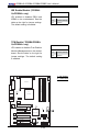
S
UPER PDSBA+
®
Processor
JP WA KE
4-PinPWR
KB/MS
USB3/4/5/6
USB1/2
LAN
Fan3
Clock
Intel
North Bridge
PCI-E x1
PCI-E x16
PCI-E x4
PCI-33MHz
LAN
CTRL
JPL 1
COM2
FWH
JL1
JWOR
I-SATA0
I-SATA1
FP C TRL
Fan2
Buzzer
24 - P in ATX P WR
Super IO
Fan1/CPU Fan
Intel
J44
DIMM#1 A ( Bl ue)
DIMM#2A (B la ck )
DIMM#1 B ( Bl ue)
DIMM#2B (B la ck )
Fl opp y
Audio
WOL
JBT1
South Bridge
J12
Battery
JPUSB1
JP U SB 2
COM1
JFSB1
JFSB2
Slot7
Slot6
Slot5
Slot4
JI
2
C1
JI
2
C2
PCI-33MHz
Slot3
PCI-33MHz
Slot2
Slot1
PCI-33MHz
J9
I-SATA4
I-SATA5
RAIDLED
USB7/8
J45
USB9/10
LE1
JLED
JWD
CD1
Parallel Port
VG A
HDA
ID E #2
ID E #1
ITE
JP2
JP3
Floppy Connector
The oppy connector is located at
J27. See the table below for pin
denitions.
Floppy Drive Connector
PinDenitions(Floppy)
Pin# Denition Pin # Denition
1 Ground 2 FDHDIN
3 Ground 4 Reserved
5 Key 6 FDEDIN
7 Ground 8 Index
9 Ground 10 Motor Enable
11 Ground 12 Drive Select B
13 Ground 14 Drive Select B
15 Ground 16 Motor Enable
17 Ground 18 DIR
19 Ground 20 STEP
21 Ground 22 Write Data
23 Ground 24 Write Gate
25 Ground 26 Track 00
27 Ground 28 Write Protect
29 Ground 30 Read Data
31 Ground 32 Side 1 Select
33 Ground 34 Diskette
A
A. Floppy