
Data Sheet
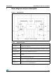

VNH3SP30-E Block diagram and pins description
7/33
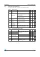
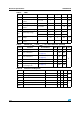
Table 4. Pin functions description
Name Description
V
CC
Battery connection
GND
A
, GND
B
Power grounds; must always be externally connected together
OUT
A
,
OUT
B
Power connections to the motor
IN
A
,
IN
B
Voltage controlled input pins with hysteresis, CMOS compatible. These two pins
control the state of the bridge in normal operation according to the truth table (brake
to V
CC
, brake to GND, clockwise and counterclockwise).
PWM
Voltage controlled input pin with hysteresis, CMOS compatible. Gates of low side
FETs are modulated by the PWM signal during their ON phase allowing speed
control of the motor.
EN
A
/DIAG
A
,
EN
B
/DIAG
B
Open drain bidirectional logic pins. These pins must be connected to an external pull
up resistor. When externally pulled low, they disable half-bridge A or B. In case of
fault detection (thermal shutdown of a high side FET or excessive ON state voltage
drop across a low side FET), these pins are pulled low by the device (see truth table
in fault condition).