
Data Sheet

VNH3SP30-E Application information
21/33
Possible origins of fault conditions may be:
● OUT
A
is shorted to ground overtemperature detection on high side A.
● OUT
A
is shorted to V
CC
low side power MOSFET saturation detection
(a)
.
When a fault condition is detected, the user can know which power element is in fault by
monitoring the IN
A
, IN
B
, DIAG
A
/EN
A
and DIAG
B
/EN
B
pins.
In any case, when a fault is detected, the faulty leg of the bridge is latched off. To turn on the
respective output (OUT
X
) again, the input signal must rise from low to high level.
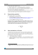
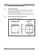
3.1 Reverse battery protection
Three possible solutions can be considered:
1. a Schottky diode
D
connected to V
CC
pin
2. an N-channel MOSFET connected to the GND pin (see Figure 33: Typical application
circuit for DC to 10 kHz PWM operation short circuit protection on page 20
3. a P-channel MOSFET connected to the V
CC
pin
The device sustains no more than -30A in reverse battery conditions because of the two
body diodes of the power MOSFETs. Additionally, in reverse battery condition the I/Os of
VNH3SP30-E will be pulled down to the V
CC
line (approximately -1.5V). A series resistor
must be inserted to limit the current sunk from the microcontroller I/Os. If I
Rmax
is the
maximum target reverse current through µC I/Os, the series resistor is:
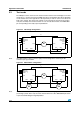
3.2 Open load detection in Off mode
It is possible for the microcontroller to detect an open load condition by adding a simply
resistor (for example, 10k ohm) between one of the outputs of the bridge (for example,
OUT
B) and one microcontroller input. A possible sequence of inputs and enable signals is
the following: IN
A = 1, INB = X, ENA = 1, ENB = 0.
● normal condition: OUTA = H and OUTB = H
● open load condition: OUTA = H and OUTB = L: In this case the OUTB pin is internally
pulled down to GND. This condition is detected on OUT
B pin by the microcontroller as
an open load fault.
a. An internal operational amplifier compares the Drain-Source MOSFET voltage with the internal reference (2.7V
Typ.). The relevant low side power MOS is switched off when its Drain-Source voltage exceeds the reference
voltage.
R
V
IOs
V
CC
–
I
Rmax
---------------------------------=