X7SBL-LN1/LN2 USER’S MANUAL Revision 1.
The information in this User’s Manual has been carefully reviewed and is believed to be accurate. The vendor assumes no responsibility for any inaccuracies that may be contained in this document, makes no commitment to update or to keep current the information in this manual, or to notify any person or organization of the updates. Please Note: For the most up-to-date version of this manual, please see our web site at www.supermicro.com. Super Micro Computer, Inc.
Preface Preface About This Manual This manual is written for system integrators , PC technician and knowledgeable PC users. It provides information for the installation and use of the X7SBL® LN1/LN2 motherboard. The X7SBL-LN1/LN2 supports single Xeon 3000 sequence processor with a system bus speed of 1330 MHz/1066 MHz. The Intel Xeon 3000 sequence processor supports the 775-Land Grid Array Package that interfaces with the motherboard via an LGA775 socket.
X7SBL-LN1/LN2 User’s Manual Table of Contents Chapter 1 Introduction 1-1 Overview ......................................................................................................... 1-1 Checklist .......................................................................................................... 1-1 Contacting Supermicro .................................................................................... 1-2 X7SBL-LN1/LN2 Image ..................................................................
Table of Contents Processor Power Connector ......................................................................... 2-15 Universal Serial Bus...................................................................................... 2-16 Chassis Intrusion........................................................................................... 2-16 ATX PS/2 Keyboard and Mouse Ports ......................................................... 2-17 Serial Ports.....................................................
X7SBL-LN1/LN2 User’s Manual 3-3 Frequently Asked Questions ........................................................................... 3-4 3-4 Returning Merchandise for Service................................................................. 3-5 Chapter 4 BIOS 4-1 Introduction...................................................................................................... 4-1 4-2 Running Setup ................................................................................................
Chapter 1: Introduction Chapter 1 Introduction 1-1 Overview Checklist Congratulations on purchasing your computer motherboard from an acknowledged leader in the industry. Supermicro boards are designed with the utmost attention to detail to provide you with the highest standards in quality and performance. Please check that the following items have all been included with your motherboard. If anything listed here is damaged or missing, contact your retailer.
X7SBL-LN1/LN2 User’s Manual Contacting Supermicro Headquarters Address: Super Micro Computer, Inc. 980 Rock Ave. San Jose, CA 95131 U.S.A. Tel: +1 (408) 503-8000 Fax: +1 (408) 503-8008 Email: marketing@supermicro.com (General Information) support@supermicro.com (Technical Support) Web Site: www.supermicro.com Europe Address: Super Micro Computer B.V. Het Sterrenbeeld 28, 5215 ML 's-Hertogenbosch, The Netherlands Tel: +31 (0) 73-6400390 Fax: +31 (0) 73-6416525 Email: sales@supermicro.
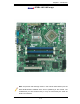
Chapter 1: Introduction X7SBL-LN1/LN2 Image Note: All pictures and drawings shown in this manual were based upon the latest PCB Revision available at the time of publishing of the manual. The motherboard you have received may or may not look exactly the same as those in this manual.
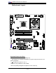
X7SBL-LN1/LN2 User’s Manual Motherboard Layout Important Notes to the User • Jumpers not indicated are for testing only. • See Chapter 2 for detailed information on jumpers, I/O ports and JF1 front panel connections. • " " indicates the location of "Pin 1." • GLAN2 is only available on LN2 models. • Slot 6 is specially designed for Supermicro riser cards only.
Chapter 1: Introduction X7SBL-LN1/LN2 Quick Reference Jumpers 2 2 JI C1/JC C2 Description Default Setting SMB to PCI Slots Open/Open (Disabled) JPF Power Force On Pins 1-2 (Reset) JPG1 VGA Enable Pins 1-2 (Enabled) JPL1/JPL2 Gigabit LAN 1/2 Enable Pins 1-2 (Enabled) JPUSB1/JPUSB2 USB 0-1 Enable/USB 2-6 Enable Pins 1-2 (Enabled) JP3 (Optional) Trusted Platform Module Enable Pins 1-2 (Enabled) JWD Watch Dog Timer Out Pins 1-2 (Reset) Connectors Description COM1 COM Port/Serial Port
X7SBL-LN1/LN2 User’s Manual Motherboard Features Processor • • • Single Intel Xeon 3000/3200 series processor with a system bus speed of 1333/1066/800 MHz Intel® Core ™ 2 Duo and Quad Processors Supports Intel Dual Core Technology, Wide Dynamic Execution, FSB Dynamic Bus Inversion (DBI), Advanced Digital Media Boost, Smart Memory Access, and Thermal Management 2 (TM2) Memory • Four DIMM slots support Dual/Single Channel DDR2 800/667 MHz up to 8 GB of ECC/Non-ECC Unbuffered DDR2 SDRAM Chipset • • In
Chapter 1: Introduction ACPI Features • • • • Slow blinking LED for suspend state indicator BIOS support for USB keyboard Main switch override mechanism Internal/external modem ring-on Onboard I/O • Intel ICH9R SATA Controller, 6 connectors for 6 devices with support of RAID functions 0, 1, 5 and 10 (RAID 5: supported by Intel's RAID Controller in the Windows OS environment only) • • • 1 floppy port interface (up to 2.
X7SBL-LN1/LN2 User’s Manual Block Diagram VID[0-7] LGA775_PROCESSOR VRM 11.0 ADDR CTRL DATA ADDR CTRL DATA S3 CK505 CLK FSB: 1333/1066/800MHz DDR2_800/667 PCIE_x8 BIGBY-V MCH 3 DIMM_CHA DIMM_CHB SLOT DMI PCI_32_BUS PCIE_x4 6 x SATA PORTS S-ATA/300 PCIE_x1 ICH-9 USB PORT_1-7 PCIE_x1 USB 2.0/1.1 2x PCI_32 PCIE_x4 SLOT 82573V GLAN 82573L GLAN PCI_32_BUS XGI - Z9S DDRII SPI LPC SPI FLASH SMBUS 4 IPMI LINK W83627HG W83793G IPMI Slot LPC I/O FDD SER.1 SER.
Chapter 1: Introduction 1-2 Chipset Overview The Intel 3200 chipset, designed for use with an Intel Xeon 3000 sequence processor in the LGA 775 Land Grid Array Package, is comprised of two primary components: the Memory Controller Hub (MCH) and the I/O Controller Hub (ICH9R). The X7SBL-LN1/LN2 provides the performance and feature-set required for the mainstream server market.
X7SBL-LN1/LN2 User’s Manual 1-3 Special Features Recovery from AC Power Loss BIOS provides a setting for you to determine how the system will respond when AC power is lost and then restored to the system. You can choose for the system to remain powered off (in which case you must hit the power switch to turn it back on) or for it to automatically return to a power- on state. See the Power Lost Control setting in the Advanced section to change this setting. (Default: Last State).
Chapter 1: Introduction I/O Virtualization Technology With the Intel ICH9R built in, the X7SBL-LN1/LN2 supports I/O Virtualization Technology (VT-d) that enables multiple operating systems and applications to run in independent partitions. Each partition uses its own subset of host physical memory, and behaves like a virtual machine (VM), providing isolation and protection across multiple partitions.
X7SBL-LN1/LN2 User’s Manual Slow Blinking LED for Suspend-State Indicator When the CPU goes into a suspend state, the chassis power LED will start blinking to indicate that the CPU is in suspend mode. When the user presses any key, the CPU will wake-up and the LED will automatically stop blinking and remain on.
Chapter 2: Installation Chapter 2 Installation 2-1 Static-Sensitive Devices Electrostatic-Discharge (ESD) can damage electronic components. To prevent damage to your system board, it is important to handle it very carefully. The following measures are generally sufficient to protect your equipment from ESD. Precautions • • Use a grounded wrist strap designed to prevent static discharge. Touch a grounded metal object before removing the board from the antistatic bag.
X7SBL-LN1/LN2 User’s Manual Note: Some components are very close to the mounting holes. Please take precautionary measures to prevent damage to these components when installing the motherboard to the chassis. 2-3 ! Processor and Heatsink Installation Warning: When handling the processor package, avoid placing direct pressure on the label area of the fan. Notes: 1. Always connect the power cord last and always remove it before adding, removing or changing any hardware components.
Chapter 2: Installation Installation of the LGA 775 Processor PnP Cap on top of the Load Plate 1. Press the load lever to release the load plate, which covers the CPU socket, from its locking position. 2. Gently lift the load lever to open the load plate. Load Plate (with PnP Cap attached) Top Center Edge 3. Use your thumb and your index finger to hold the CPU at the top center Triangle edge and the bottom center edge of the CPU. 4.
X7SBL-LN1/LN2 User’s Manual 5. Align the CPU key that is the semi-circle cutout below a golden dot against the socket key, the Notch on the same side of the triangle cutout on the socket. 6. Once aligned, carefully lower the CPU straight down to the socket. (**Do not drop the CPU on the socket. Do not move the CPU horizontally or vertically. Do not rub the CPU against the surface or against any pins of the socket to avoid damage to the CPU or the socket.) 7.
Chapter 2: Installation Installation of the Heatsink 1. Do not apply any thermal grease to the heatsink or the CPU die, the required amount has already been applied. 2. Place the heatsink on top of the CPU so that the four mounting holes are aligned with those on the retention mechanism. 3. Screw in two diagonal screws (eg. the #1 and the #2 screws) until just snug (do Screw 1 not fully tighten the screws, which may damage the CPU). Screw 2 4.
X7SBL-LN1/LN2 User’s Manual Removal of the Heatsink Warning: We do not recommend that the CPU or the heatsink be ! removed. However, if you do need to uninstall the heatsink, please follow these instructions below to prevent damage to the CPU or the CPU socket. 1. Unscrew and remove the heatsink screws from in the sequence as show in the picture on the right. 2. Hold and gently wriggle the heatsink to loosen it from the CPU. (Do not use excessive force when loosening the heatsink!) 3.
Chapter 2: Installation 2-4 Installing DIMMs Note: Check the Supermicro web site for recommended memory modules. Warning: Exercise extreme care when installing or removing DIMM modules to prevent any possible damage. Also note that ! the memory is interleaved to improve performance (see step 1). DIMM Installation 1. Insert the desired number of DIMMs into the memory slots, starting with DIMM1A.
X7SBL-LN1/LN2 User’s Manual Possible System Memory Allocation & Availability System Device Size Physical Memory Remaining (-Available) (4 GB Total System Memory) Firmware Hub flash memory (System BIOS) 1 MB 3.99 Local APIC 4 KB 3.99 Area Reserved for the chipset 2 MB 3.99 I/O APIC (4 Kbytes) 4 KB 3.99 PCI Enumeration Area 1 256 MB 3.76 PCI Express (256 MB) 256 MB 3.51 PCI Enumeration Area 2 (if needed) -Aligned on 256-MB boundary- 512 MB 3.01 VGA Memory 16 MB 2.85 TSEG 1 MB 2.
Chapter 2: Installation 2-5 Control Panel Connectors/IO Ports The I/O ports are color coded in conformance with the PC 99 specification. See the image below for the colors and locations of the various I/O ports. 1. Back Panel Connectors/IO Ports Back Panel I/O Port Locations and Definitions 2 4 5 3 1 Back Panel Connectors 1. Keyboard (Purple) 2. PS/2 Mouse (Green) 3. Back Panel USB Port 0 4. Back Panel USB Port 1 5. COM Port 1 (Turquoise) 6. VGA Port (Blue) 7. Gigabit LAN 1 8.
X7SBL-LN1/LN2 User’s Manual 2. Front Control Panel JF1 contains header pins for various buttons and indicators that are normally located on a control panel at the front of the chassis. See the image below for the descriptions of the various control panel buttons and LED indicators. Refer to the following section for descriptions and pin definitions. A.
Chapter 2: Installation 3. Front Control Panel Pin Definitions NMI Button NMI Button Pin Definitions (JF1) The non-maskable interrupt button header is located on pins 19 and 20 of JF1. Refer to the table on the right Pin# Definition 19 Control 20 Ground for pin definitions. Power LED Power LED Pin Definitions (JF1) The Power LED connection is located on pins 15 and 16 of JF1. Refer to the table on the right for pin definitions. Pin# Definition 15 +5V 16 Ground A. NMI B.
X7SBL-LN1/LN2 User’s Manual NIC1/NIC2 LED Indicators The NIC (Network Interface Controller) LED connection for GLAN 1 is located on pins 11 and 12 of JF1 and the LED connection for GLAN 2 is on GLAN 1 LED Pin Definitions (JF1) GLAN 2 LED Pin Definitions (JF1) Pin# Pin# Definition Definition 11 LED_Anode+ 9 LED_Anode+ 12 NIC1 LED Signal 10 NIC1 LED Signal Pins 9 and 10. Attach the NIC LED cables to display network activity. Refer to the table on the right for pin definitions.
Chapter 2: Installation Overheat/Fan Fail LED (OH) OH/Fan Fail Indicator Status Connect an LED to the OH/Fan State Fail connection on pins 7 and 8 of JF1 to provide advanced warning of chassis overheating or fan failure. Refer to the table on the right for pin Definition Off Normal On Overheat Flashing Fan Fail definitions. Power Fail LED The Power Fail LED connection is PWR Fail LED Pin Definitions (JF1) located on pins 5 and 6 of JF1.
X7SBL-LN1/LN2 User’s Manual Reset Button Reset Button Pin Definitions (JF1) The Reset Button connection is located on pins 3 and 4 of JF1. Attach it to the hardware reset switch on the computer case. Refer to the table on the right for Pin# Definition 3 Reset 4 Ground pin definitions. Power Button The Power Button connection is located on pins 1 and 2 of JF1.
Chapter 2: Installation 2-6 Connecting Cables ATX Power Connector ATX Power 24-pin Connector Pin Definitions There are a 24-pin main power supply connector(JPW1) and an 8-pin CPU PWR connector (JPW2) on the motherboard. These power connectors meet the SSI EPS 12V specification. For the 8-pin PWR (JPW2), please refer to the item listed below. Processor Power Connector Pin# Definition Pin # Definition 13 +3.3V 1 +3.3V 14 -12V 2 +3.
X7SBL-LN1/LN2 User’s Manual Universal Serial Bus (USB) Back Panel USB (J15) There are seven USB 2.0 (Universal Serial Bus) ports/headers on the motherboard. Two of them are Back Panel USB ports (USB 0-1: J15). Another two USB Headers: (USB 2-3: J44) and (USB 4-5 : J45) can provide front access USB connections. (FP USB 6: J47) is a front panel USB con- Pin# Definitions 1 +5V 2 PO- 3 PO+ 4 Ground 5 N/A Front Panel & Front Accessible USB Pin Definitions (J44, J45, J47) nection.
Chapter 2: Installation ATX PS/2 Keyboard and PS/2 Mouse Ports PS/2 Keyboard and Mouse Port Pin Definitions The ATX PS/2 keyboard and the PS/2 Pin# Definition mouse are located at J28. See the 1 Data 2 NC 3 Ground 4 VCC 5 Clock 6 NC table on the right for pin definitions. (The mouse port is above the keyboard port. See the table on the right for pin definitions.
X7SBL-LN1/LN2 User’s Manual Power LED PWR LED Pin Definitions The Power LED connector is located at JLED. This connection is used to provide LED Indication of power being supplied to the system. See the table on the right for pin definitions.
Chapter 2: Installation GLAN (Giga-bit Ethernet Ports) Two G-bit Ethernet ports (GLAN1/ GLAN2) are located next to the VGA GLAN1 GLAN2 Connector on the IO backplane. These ports accept RJ45 type cables. VGA Connector A VGA connector (J16) is located between COM1 and GLAN1 on the IO backplane. Refer to the board layout below for the location. A. GLAN1 B. GLAN2 C.
X7SBL-LN1/LN2 User’s Manual Fan Headers 4-pin Fan Header Pin Definitions (Fan1-6) The X7SBL-LN1/LN2 has six fan headers (Fan1 to Fan6) including five chassis/sys- Pin# Definition tem fan headers (Fan1 to Fan5) and one 1 Ground CPU Fan (CPU Fan6). All these fan head- 2 +12V ers support 4-pin fans. However, Pins 1-3 3 Tachometer of the fan headers are backward compat- 4 PWR Modulation ible with the traditional 3-pin fans. See the table on the right for pin definitions.
Chapter 2: Installation Wake-On-Ring Wake-On-Ring Pin Definitions (JWOR) The Wake-On-Ring header is located at JWOR. This feature allows your computer to be awakened by an incoming call to the modem when the system is in the suspend state. See the table Pin# Definition 1 Ground 2 Wake-up on the right for pin definitions. You must have a Wake-On-Ring card and a cable to use this feature. Wake-On-LAN Wake-On-LAN Pin Definitions (JWOL) The Wake-On-LAN header is located at JWOL on the motherboard.
X7SBL-LN1/LN2 User’s Manual Power Fault (PWR Supply Failure) PWR Supply Fail Pin Definitions Connect a cable from your power supply to the Power Fail (PW3) header to provide a warning in the event of a power supply failure. This warning signal is passed through the PWR_LED Pin# Definition 1 PWR 1: Fail 2 PWR 2: Fail 3 PWR 3: Fail 4 Signal: Alarm Reset pin to indicate of a power failure on the chassis.
Chapter 2: Installation 2-7 Jumper Settings Explanation of Jumpers To modify the operation of the motherboard, jumpers can be used to choose between optional settings. Jumpers create shorts between two pins to change the function of the connector. Pin 1 is identified with a square solder pad on the printed circuit board. See the motherboard layout pages for jumper locations. Note: On two pin jumpers, "Closed" means the jumper is on and "Open" means the jumper is off the pins.
X7SBL-LN1/LN2 User’s Manual Clear CMOS JBT1 is used to clear CMOS. Instead of pins, this "jumper" consists of contact pads to prevent the accidental clearing of CMOS. To clear CMOS, use a metal object such as a small screwdriver to touch both pads at the same time to short the connection. Always remove the AC power cord from the system before clearing CMOS. Note: For an ATX power supply, you must completely shut down the system, remove the AC power cord and then close pins 1 and 2 to clear CMOS.
Chapter 2: Installation PCI/PCI-E Slots to SMB Speeds SMBus to PCI-X/PCI-Exp Slots Jumper Settings Jumpers JI2C1/JI2C2 allow you to connect PCI/PCI-Exp. Slots to the System Management Bus. The de- Jumper Setting Definition Closed Enabled Open Disabled (*Default) fault setting is open to disable the connection. See the table on the right for jumper settings. VGA Enable/Disable VGA Enable JPG1 enables or disables the VGA Connector on the motherboard.
X7SBL-LN1/LN2 User’s Manual Force-Power-On Enable/Disable Jumper JPF allows you to enable or disable the function of Force-Power-On. If enabled, the power will always stay on automatically. If this function is disabled, the user needs to press the Power Force On Jumper Settings Pin# Definition Off Normal On Force On power button to power on the system. A.
Chapter 2: Installation USB Wake-Up JPUSB2 (Front Panel USB Wake-up) Use JPUSB jumpers to enable the function of "System Wake-Up via USB devices", which allows you to "wake-up" the system by pressing a key on the USB keyboard or by clicking the USB Pin# Definition 1-2 Enabled 2-3 Disabled (*default) mouse of your system. The JPUSB jumpers are used together with the USB Wake-Up function in the BIOS.
X7SBL-LN1/LN2 User’s Manual 2-8 Onboard Indicators GLAN LEDs Link Activity LED LED There are two GLAN ports on the motherboard. Each Gigabit Ether- (*Rear View: When viewing it from net LAN port has two LEDs. The the rear side of the chassis) yellow LED indicates activity, while the Link LED may be green, amber GLAN Activity Indicator or off to indicate the speed of the connection. See the tables at right for more information.
Chapter 2: Installation Onboard Power LED (LE1) Onboard PWR LED Indicator (LE1) The Onboard 3.3V Standby Power LED is located at LE1 on the motherboard. When LE1 is off, the system is off. When the LED is on, LED Color Definition Off System Off On Standby Power On Green System On the power is on. Unplug the power cable before removing or installing components. See the layout below for the LED location. A.
X7SBL-LN1/LN2 User’s Manual 2-9 Floppy and SIM 1U IPMI Connections Note the following when connecting the floppy and hard disk drive cables: • The floppy disk drive cable has seven twisted wires. • A red mark on a wire typically designates the location of pin 1. • A single floppy disk drive ribbon cable has two connectors to provide for two floppy disk drives. The connector with twisted wires always connects to drive A, and the connector that does not have twisted wires always connects to drive B.
Chapter 2: Installation SIM 1U IPMI A SIM 1U IPMI Socket is located at J19 on the motherboard. This connection provides IPMI (Intelligent Power Management Interface) capability to the motherboard. Refer to the layout below for the SIM 1U IPMI location. A.
X7SBL-LN1/LN2 User’s Manual Notes 2-32
Chapter 3: Troubleshooting Chapter 3 Troubleshooting 3-1 Troubleshooting Procedures Use the following procedures to troubleshoot your system. If you have followed all of the procedures below and still need assistance, refer to the ‘Technical Support Procedures’ and/or ‘Returning Merchandise for Service’ section(s) in this chapter. Always disconnect the AC power cord before adding, changing or installing any hardware components. Before Power On 1.
X7SBL-LN1/LN2 User’s Manual 3. Check that the 115V/230V switch on the power supply is properly set. 4. Turn the power switch on and off to test the system. 5. The battery on your motherboard may be old. Check to verify that it still supplies ~3VDC. If it does not, replace it with a new one. No Video 1. If the power is on but you have no video, remove all the add-on cards and cables. 2. Use the speaker to determine if any beep codes exist. Refer to Appendix A for details on beep codes.
Chapter 3: Troubleshooting 3. If the above steps do not fix the Setup Configuration problem, contact your vendor for repairs. 3-2 Technical Support Procedures Before contacting Technical Support, please take the following steps. Also, note that as a motherboard manufacturer, Super Micro does not sell directly to end-users, so it is best to first check with your distributor or reseller for troubleshooting services.
X7SBL-LN1/LN2 User’s Manual 3-3 Frequently Asked Questions Question: What type of memory does my motherboard support? Answer: The X7SBL-LN1/LN2 supports unbuffered, ECC/Non-ECC DDR2 667/800 MHz memory modules. See Section 2-4 for details on installing memory. Question: Why does Microsoft Windows XP (SP2) and Windows Vista show less memory than what is physically installed? Answer: Microsoft implemented a design change in Windows XP with Service Pack 2 (SP2) and Windows Vista.
Chapter 3: Troubleshooting Question: After I have installed 4 pieces of 1GB Memory, why does the BIOS only detect about 3.145 GB of memory during POST? Answer: Because the chipset does not support memory remapping, and PCI-E memory requires a great deal of memory, so there is a memory hole located around the 4GB memory address. 3-4 Returning Merchandise for Service A receipt or copy of your invoice marked with the date of purchase is required before any warranty service will be rendered.
X7SBL-LN1/LN2 User’s Manual Notes 3-6
Chapter 4: BIOS Chapter 4 BIOS 4-1 Introduction This chapter describes the Phoenix BIOS™ Setup utility for the X7SBL-LN1/LN2. The Phoenix ROM BIOS is stored in a flash chip and can be easily upgraded using a floppy disk-based program. Note: Due to periodic changes to the BIOS, some settings may have been added or deleted and might not yet be recorded in this manual. Please refer to the Manual Download area of the Super Micro web site
X7SBL-LN1/LN2 User's Manual 4-2 Running Setup *Default settings are in bold text unless otherwise noted. The BIOS setup options described in this section are selected by choosing the appropriate text from the main BIOS Setup screen. All displayed text is described in this section, although the screen display is often all you need to understand how to set the options (see next page). When you first power on the computer, the Phoenix BIOS™ is immediately activated.
Chapter 4: BIOS Main BIOS Setup Menu uMain Setup Features System Time To set the system date and time, key in the correct information in the appropriate fields. Then press the key to save the data. System Date Using the arrow keys, highlight the month, day and year fields, and enter the correct data. Press the key to save the data. Legacy Diskette A This setting allows the user to set the type of floppy disk drive installed as diskette A. The options are Disabled, 360Kb 5.25 in, 1.2MB 5.
X7SBL-LN1/LN2 User's Manual BIOS Date The item displays the date that the BIOS was built. BIOS Revision The item displays the BIOS revision number. Hard Disk Pre-Delay This setting allows the user to add a delay prior to the first access of a hard disk by the BIOS. The delay ensures that the hard disk has time to initialize before power up.
Chapter 4: BIOS SATA AHCI Legacy Enable This setting allows you to disable SATA ports 5 and 6 while in this mode. The options are Disabled and Enabled. uIDE Channel 0 Master/Slave/SATA Port2/SATA Port3 These settings allow you to set the parameters of slots indicated above. Hit to activate the following sub-menu screen for detailed options of these items. Set the correct configurations accordingly.
X7SBL-LN1/LN2 User's Manual CHS Format The following items will be displayed by the BIOS: TYPE: This item displays the type of IDE or SATA Device. Cylinders: This item indicates the status of Cylinders. Headers: This item indicates the number of headers. Sectors: This item displays the number of sectors. Maximum Capacity: This item displays the maximum storage capacity of the system.
Chapter 4: BIOS 32 Bit I/O This option allows you to enable or disable the function of a 32-bit data transfer. The options are Enabled and Disabled. Transfer Mode This option allows you to set the transfer mode. The options are Standard, Fast PIO1, Fast PIO2, Fast PIO3, Fast PIO4, FPIO3/DMA1 and FPIO4/DMA2. Ultra DMA Mode This option allows you to select the Ultra DMA Mode. The options are Disabled and Enabled.
X7SBL-LN1/LN2 User's Manual 4-4 Advanced Setup Choose Advanced from the Phoenix BIOS Setup Utility main menu with the arrow keys. You should see the following display. The items with a triangle beside them have sub- menus that can be accessed by highlighting the item and pressing . uBoot Features Quiet Boot This setting allows you to Enable or Disable the graphic logo screen display during bootup.
Chapter 4: BIOS POST Errors Use the setting to Pause and Display SETUP entry or resume boot prompt if error occurs on boot disabled. The options are Enabled and Disabled. ACPI Mode Use the setting to determine whether you want to use the ACPI (Advanced Configuration and Power Interface) power management on your system. The options are Yes and No. Power Button Behavior If set to Instant-Off, the system will power on or power off immediately as soon as you hit the power button.
X7SBL-LN1/LN2 User's Manual Power Loss Control This setting allows you to choose how the system will react when power returns after an unexpected loss of power. The options are Stay Off, Power On, and Last State. Watch Dog Select Enabled to automatically reset the system if the system is not active for more than 4 minutes. The options are Enabled and Disabled. Summary Screen This setting allows you to Enable or Disable the summary screen which displays the system configuration during bootup.
Chapter 4: BIOS Hyperthreading (Available when supported by the CPU) Set to Enabled to use the Hyperthreading Technology, which will result in increased CPU performance. The options are Enabled and Disabled. Core-Multi-Processing (Available when supported by the CPU.) Set to Enabled to use a processor's Second Core and beyond. (Please refer to Intel's web site for more information.) The options are Disabled and Enabled.
X7SBL-LN1/LN2 User's Manual Adjacent Cache Line Prefetch (*Available when supported by the CPU.) The CPU fetches the cache line for 64 bytes if this option is set to Disabled. The CPU fetches both cache lines for 128 bytes as comprised if Enabled. The options are Disabled and Enabled.. Set Maximum Ext. CPUID=3 When set to Enabled, the Maximum Extended CPUID will be set to 3. The options are Disabled and Enabled. Echo TPR Set to Enabled to prevent xTPR messages from being sent to the system.
Chapter 4: BIOS No Execute Mode Memory Protection (Available when supported by the CPU and the OS.) Set to Enabled to enable Execute Disable Bit and allow the processor to classify areas in memory where an application code can execute and where it cannot, and thus preventing a worm or a virus from inserting and creating a flood of codes to overwhelm the processor or damage the system during an attack. Note 1: This feature is available when your OS and your CPU support the function of Execute Disable Bit.
X7SBL-LN1/LN2 User's Manual Memory Remapping This feature allows the bios reserve memories to remap the memory above the 4GB to 5GB area when using 4GB of memory. The settings are Enabled and Disabled. Enable VT-D Select Enable to use the functionality of VT-D. The options are Enabled and Disabled.
Chapter 4: BIOS uMemory Cache Cache System BIOS Area This setting allows you to designate a reserve area in the system memory to be used as a System BIOS buffer and allow BIOS to write (cache) data into this reserved memory area. Select Write Protect to enable this function, and this area will be reserved for BIOS ROM access only. Select Uncached to disable this function and make this area available for other devices.
X7SBL-LN1/LN2 User's Manual to write data back directly from the buffer without writing data to the System Memory for fast CPU. Cache Extended Memory If enabled, this feature will allow the data stored in the extended memory area to be cached (written) into a buffer, a storage area in the Static DROM (SDROM) or written into L1, L2, L3 cache inside the CPU to speed up CPU operations. Select Uncached to disable this function.
Chapter 4: BIOS 0020h, 0040h, 0060h, 0080h, 00A0h, 00C0h, and 00E0h. For Unix, Novell and other Operating Systems, please select the option: other. If a drive fails after the installation of a new software, you might want to change this setting and try again. A different OS requires a different Bus Master clock rate. uSlot 3 PCI-Exp x4 Access the submenu for each of the settings above to make changes to the following: Option ROM Scan When enabled, this setting will initialize the device expansion ROM.
X7SBL-LN1/LN2 User's Manual Enable Master This setting allows you to enable the selected device as the PCI bus master. The options are Enabled and Disabled. Latency Timer This setting allows you to set the clock rate for Bus Master. A high-priority, highthroughout device may benefit from a greater clock rate. The options are Default, 0020h, 0040h, 0060h, 0080h, 00A0h, 00C0h, and 00E0h. For Unix, Novelle and other Operating Systems, please select the option: other.
Chapter 4: BIOS KBC Clock Input This setting allows you to select the clock frequency for the Keyboard Controller. The options are 6MHz, 8MHz, 12MHz, and 16MHz. Serial Port A This setting allows you to decide how the system controls Serial Port A. The options are Enabled (user defined) and Disabled. Base I/O Address This setting allows you to select the base I/O address for Serial Port A. The options are 3F8, 2F8, 3E8, and 2E8.
X7SBL-LN1/LN2 User's Manual Interrupt This setting allows you to select the IRQ (interrupt request) for Serial Port B. The options are IRQ3 and IRQ4. Floppy Disk Controller This setting allows you to assign control of the floppy disk controller. The options are Enabled (user defined), Disabled, and Auto (BIOS and OS controlled). uDMI Event Logging Event Log Validity This displays the validity of the DMI event log. Event Log Capacity This displays the space available in the DMI event log.
Chapter 4: BIOS uConsole Redirection Access the submenu to make changes to the following settings: COM Port Address This setting will allow you to specify which COM port to direct the remote console to: Onboard COM A or Onboard COM B. The options are Disabled, COM A and COM B. Baud Rate This setting will enable you to set the BAUD rate for the console redirection. The options are 300,1200, 2400, 9600, 19.2 K, 38.4K, 57.6K, and 115.2K.
X7SBL-LN1/LN2 User's Manual CPU Overheat Alarm This option allows the user to select the CPU Overheat Alarm setting which determines when the CPU OH alarm will be activated to provide warning of possible CPU overheat. Warning: Any temperature that exceeds the CPU threshold temperature predefi ned by the CPU manufacturer may result in CPU overheat or system instability. When the CPU temperature reaches this predefi ned threshold, the CPU and system cooling fans will run at full speed.
Chapter 4: BIOS CPU Temperature The item displays the level of CPU temperature (High, Medium, Low) as detected by the BIOS. The information shown in the screen is for your reference only. (See the notes below for more information on DTS and PECI) Low – This level is considered as the ‘normal’ operating temperature. No action is required. The PECI count is below or equal to the processor’s DTS thermal throttle point, minus 10 PECI counts. Medium – The processor is running warmer.
X7SBL-LN1/LN2 User's Manual provide PECI counts as references for fan speed controls. So all our Intel processor-based motherboards will be/have been updated to change the CPU temperature display from numbers (absolute temperatures) to text (low, medium, and high). Each processor has a DTS and every processor’s DTS is individually calibrated at the factory. DTS’ function is to provide digital data that informs the system of the processor’s thermal throttle point.
Chapter 4: BIOS 3-pin (server) 3-pin (workstation), 4-pin (server) and 4-pin (workstation). Do not select 4-pin settings if you have a mix of 3-pin and 4-pin fans. Voltage Monitoring The following items will be monitored and displayed: Vcore A, MCH Core, -12V, V-DIMM, 3.3V, +12V, 5V Standby, 5VDD, PVTT, Vbatt Note: In the Windows OS environment, the Supero Doctor III settings take precedence over the BIOS settings.
X7SBL-LN1/LN2 User's Manual Supervisor Password Is: This item indicates if a supervisor password has been entered for the system. Clear means such a password has not been used and Set means a supervisor password has been entered for the system. User Password Is: This item indicates if a user password has been entered for the system. Clear means such a password has not been used and Set means a user password has been entered for the system.
Chapter 4: BIOS 4-6 Boot Settings Choose Boot from the Phoenix BIOS Setup Utility main menu with the arrow keys. You should see the following display. See details on how to change the order and specs of boot devices in the Item Specific Help window. All Boot BIOS settings are described in this section. Boot List Candidate List Boot Priority Order/Excluded from Boot Orders The devices included in the boot list section (above) are bootable devices listed in the sequence of boot order as specified.
X7SBL-LN1/LN2 User's Manual 4-7 Exit Choose Exit from the Phoenix BIOS Setup Utility main menu with the arrow keys. You should see the following display. All Exit BIOS settings are described in this section. Exit Saving Changes Highlight this item and hit to exit the BIOS Setup utility while saving any changes you may have made. Exit Discarding Changes Highlight this item and hit to exit the BIOS Setup utility without saving any changes you may have made.
Chapter 4: BIOS Discard Changes Highlight this item and hit to discard (cancel) any changes you made. You will remain in the Setup utility. Save Changes Highlight this item and hit to save any changes you made. You will remain in the Setup utility.
X7SBL-LN1/LN2 User's Manual Notes 4-30
Appendix A: BIOS POST Messages Appendix A BIOS Error Beep Codes This section lists POST (Power On Self Test) error beep codes for the Phoenix BIOS. POST error beep codes are divided into two categories: recoverable and terminal. This section lists Beep Codes for recoverable POST errors. Recoverable POST Error Beep Codes When a recoverable type of error occurs during POST, BIOS will display a POST code that describes the problem.
X7SBL-LN1/LN2 User's Manual Notes A-2
Appendix B: BIOS POST Codes Appendix B Installing the Windows OS After all hardware components have been installed, you must first configure Intel South Bridge RAID Settings before you install the Windows OS and other software drivers. To configure RAID settings, please refer to RAID Configuration User Guides posted on our website at www.supermicro.com/support/manuals. B-1 Installing the Windows XP/2000/2003 OS for Systems with RAID Functions 1.
X7SBL-LN1/LN2 User's Manual B-2 Installing the Windows XP/2000/2003 OS for Systems without RAID Functions 1. Insert Microsoft's Windows XP/2000/2003 Setup CD in the CD Driver, and the system will start booting up from CD. 2. Continue with the OS installation. The Windows OS Setup screen will display. 3. From the Windows XP/2000/2003 Setup screen, press the key. The XP/2000/2003 Setup will automatically load all device files and then continue with the Windows XP/2000/2003 installation. 4.
Appendix C: Intel HostRAID Setup Guidelines Appendix C Installing Other Software Programs and Drivers C-1 Installing Drivers other than the Adaptec Embedded Serial ATA RAID Controller Driver After you've installed the Windows Operating System, a screen as shown below will appear. You are ready to install software programs and drivers that have not yet been installed. To install these software programs and drivers, click the icons to the right of these items.
X7SBL-LN1/LN2 User's Manual C-2 Configuring Supero Doctor III The Supero Doctor III program is a Web-base management tool that supports remote management capability. It includes Remote and Local Management tools. The local management is called the SD III Client. The Supero Doctor III program included on the CDROM that came with your motherboard allows you to monitor the environment and operations of your system.
Appendix C: Intel HostRAID Setup Guidelines Supero Doctor III Interface Display Screen-II (Remote Control) Note: SD III Software Revision 1.0 can be downloaded from our website at: ftp://ftp.supermicro.com/utility/Supero_Doctor_III/. You can also download SDIII User's Guide at: http://www.supermicro.com/PRODUCT/ Manuals/SDIII/UserGuide.pdf. For Linux, we will still recommend that you use Supero Doctor II.
X7SBL-LN1/LN2 User's Manual Notes C-4
Disclaimer The products sold by Supermicro are not intended for and will not be used in life support systems, medical equipment, nuclear facilities or systems, aircraft, aircraft devices, aircraft/emergency communication devices or other critical systems whose failure to perform be reasonably expected to result in significant injury or loss of life or catastrophic property damage.