SUPER ® SUPER X5DL8-GG SUPER X5DLR-8G2+ SUPER X5DLR-8G2 USER’S MANUAL Revision 1.
The information in this User’s Manual has been carefully reviewed and is believed to be accurate. The vendor assumes no responsibility for any inaccuracies that may be contained in this document, makes no commitment to update or to keep current the information in this manual, or to notify any person or organization of the updates. Please Note: For the most up-to-date version of this manual, please see our web site at www.supermicro.com.
Preface Preface About This Manual This manual is written for system integrators, PC technicians and knowledgeable PC users. It provides information for the installation and use of the SUPER X5DL8-GG/X5DLR-8G2+/X5DLR-8G2 serverboard. At launch, the SUPER X5DL8-GG/X5DLR-8G2+/X5DLR-8G2 supported single or dual Intel® XeonTM 1.50 - 3.20 GHz processors at a 533/400 MHz front side bus. Refer to the motherboard specifications pages on our web site ( http:// www.supermicro.com/Product_page/product-m.
SUPER X5DL8-GG/X5DLR-8G2+/X5DLR-8G2 User’s Manual Table of Contents Preface About This Manual ...................................................................................................... iii Manual Organization ................................................................................................... iii Chapter 1: Introduction 1-1 Overview ......................................................................................................... 1-1 Checklist ...........................
Table of Contents HDD LED .................................................................................................... 2-9 NIC1 LED ................................................................................................... 2-9 NIC2 LED ................................................................................................... 2-9 Overheat LED ........................................................................................... 2-9 Power Fail LED ..............................
SUPER X5DL8-GG/X5DLR-8G2+/X5DLR-8G2 User’s Manual PCI-X Bus Speed Setting (X5DLR-8G2/X5DLR-8G2+) ...................... 2-19 33 MHz PCI Enable/Disable ................................................................... 2-19 Front Side Bus Speed ........................................................................... 2-20 Spread Spectrum .................................................................................... 2-20 PCI 3.3V Standby Enable/Disable ................................................
Chapter 1: Introduction 1-1 Introduction Chapter 1 Introduction Overview Checklist Congratulations on purchasing your computer motherboard from an acknowledged leader in the industry. Supermicro boards are designed with the utmost attention to detail to provide you with the highest standards in quality and performance. Please check that the following items have all been included with your motherboard. If anything listed here is damaged or missing, contact your retailer.
SUPER X5DL8-GG/X5DLR-8G2+/X5DLR-8G2 User’s Manual Contacting Supermicro Introduction Headquarters Address: Tel: Fax: Email: Web Site: SuperMicro Computer, Inc. 980 Rock Ave. San Jose, CA 95131 U.S.A. +1 (408) 503-8000 +1 (408) 503-8008 marketing@supermicro.com (General Information) support@supermicro.com (Technical Support) www.supermicro.com Europe Address: Tel: Fax: Email: SuperMicro Computer B.V.
Chapter 1: Introduction Introduction Notes 1-3
SUPER X5DL8-GG/X5DLR-8G2+/X5DLR-8G2 User’s Manual Figure 1-1.
Figure 1-2. SUPER X5DLR-8G2 Image Note: the X5DLR-8G2+ has the same layout but has 1) no parallel (printer) port and 2) a standard PCI-X slot.
SUPER X5DL8-GG/X5DLR-8G2+/X5DLR-8G2 User’s Manual Introduction Figure 1-3.
Chapter 1: Introduction Jumper J29 J35 JA4 JBT1 JP2 JP3 JP4 JP7 JP12 JP48 JP54 JP56 JP58 JPA1/A2 P1/2, S1/2 Description 33 MHz PCI Enable/Disable Spread Spectrum SCSI Enable/Disable CMOS Clear PCI 3.
SUPER X5DL8-GG/X5DLR-8G2+/X5DLR-8G2 User’s Manual Introduction Figure 1-4.
Chapter 1: Introduction Jumper J35 JA4 JBT1 JP2 JP3 JP12 JP48 JP56 JP58 JPA1/A2 P2 Description Spread Spectrum SCSI Enable/Disable CMOS Clear Speaker Enable/Disable Watch Dog System Bus Speed Chassis/Overheat Fan Select VGA Enable/Disable Fan Detection Select SCSI Channel A/B Termination PCI-X Speed Settings Connector ATX POWER BANK1A-BANK3B COM1/COM2 CPU1/CPU2 CPU/CHS/OH FAN D1-D8 GLAN1/GLAN2 J1 J11 J12 J18, J19 J51 J56 J64 J65 JA1/JA2 JF1 JP46 JP57 USB0/1 USB2/3 VGA Default Setting Open (Disabled) Pin
SUPER X5DL8-GG/X5DLR-8G2+/X5DLR-8G2 User’s Manual Motherboard Features Introduction CPU • Single or dual Intel ® Xeon TM 1.50 - 3.20 GHz 604/603-pin processors with a 1 MB cache at a front side (system) bus speed of 533/400 MHz. Note: Please refer to the motherboard specifications pages on our web site for updates on supported processors (http://www.supermicro.com/Product_page/product-m.htm).
Chapter 1: Introduction ACPI Features • Slow blinking LED for suspend state indicator • Main switch override mechanism • External modem ring-on Onboard I/O • AIC-7902 for dual channel Ultra320 SCSI • Adaptec 2010S SCSI RAID support (X5DL8-GG) • Adaptec 2015S SCSI RAID support (X5DLR-8G2+/X5DLR-8G2) • Integrated ATI Rage XL Graphics Controller • Intel 82540EM Gb Ethernet controller (X5DL8-GG - LAN1) • Broadcom BCM5703 Gb Ethernet controller (X5DL8-GG - LAN2) • Broadcom BCM5704 dual Gb Ethernet controller (
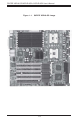
SUPER X5DL8-GG/X5DLR-8G2+/X5DLR-8G2 User’s Manual Introduction ATIXL VG A PCIBus PC I-X Slots #4,5 Processor 1 LAN1 ATA 100 Ports USB Ports Processor 0 CSB5 (South Bridge) S2 533/400 M Hz Host Bus Thin IM B North Bridge (CM IC-W S) IM B BUS C IO BX2 (IO Bridge) LAN2 PCI-X Slot #6 SM Bus IM B BUS LPC Bus SerialPort P2 SIO 266/200 M Hz M em ory Bus S1 C IO BX2 (IO Bridge) Parallel Port SC SI PCI-X Slot #1 P1 Floppy Port DDR-266 SDRAM PC I-X Slots #2,3 Figure 1-5 .
Chapter 1: Introduction Chipset Overview The ServerWorks Grand Champion LE TM is a high-performance work station SystemSet core logic chipset that consists of a North Bridge, a South Bridge and an IO bridge. The North Bridge interfaces directly to the processor bus and integrates the functions of the main memory subsystem and the IMB bus interface unit.
SUPER X5DL8-GG/X5DLR-8G2+/X5DLR-8G2 User’s Manual on state. See the Power Lost Control setting in the Advanced BIOS Setup section (Peripheral Device Configuration) to change this setting. The default setting is Always On. Introduction 1-4 PC Health Monitoring This section describes the PC health monitoring features of the SUPER X5DL8-GG/X5DLR-8G2+/X5DLR-8G2. It has an onboard System Hardware Monitor chip that supports PC health monitoring.
Chapter 1: Introduction This feature is available when used with Intel's LANDesk Client Manager (optional). LDCM is used to notify the user of certain system events. For example, if the system is running low on virtual memory and there is insufficient hard drive space for saving the data, you can be alerted of the potential problem. Hardware BIOS Virus Protection The system BIOS is protected by hardware that prevents viruses from infecting the BIOS area.
SUPER X5DL8-GG/X5DLR-8G2+/X5DLR-8G2 User’s Manual Microsoft OnNow Introduction The OnNow design initiative is a comprehensive, system-wide approach to system and device power control. OnNow is a term for a PC that is always on but appears to be off and responds immediately to user or other requests. Slow Blinking LED for Suspend-State Indicator When the CPU goes into a suspend state, the chassis power LED will start blinking to indicate that the CPU is in suspend mode.
Chapter 1: Introduction 1-6 Power Supply As with all computer products, a stable power source is necessary for proper and reliable operation. It is even more important for processors that have high CPU clock rates. The SUPER X5DL8-GG/X5DLR-8G2+/X5DLR-8G2 accommodates ATX power supplies. Although most power supplies generally meet the specifications required by the CPU, some are inadequate.
SUPER X5DL8-GG/X5DLR-8G2+/X5DLR-8G2 User’s Manual complete modem control capability and a processor interrupt system. Each UART includes a 16-byte send/receive FIFO, a programmable baud Introduction rate generator, complete modem control capability and a processor interrupt system. Both UARTs provide legacy speed with baud rate of up to 115.2 Kbps as well as an advanced speed with baud rates of 250 K, 500 K, or 1 Mb/s, which support higher speed modems.
Chapter 2: Installation Chapter 2 Installation 2-1 Static-Sensitive Devices Electric-Static-Discharge (ESD) can damage electronic components. To prevent damage to your system board, it is important to handle it very carefully. The following measures are generally sufficient to protect your equipment from ESD. Precautions • Use a grounded wrist strap designed to prevent static discharge. • Touch a grounded metal object before removing the board from the antistatic bag.
SUPER X5DL8-GG/X5DLR-8G2+/X5DLR-8G2 User’s Manual 2-2 PGA Processor and Heatsink Installation ! When handling the processor package, avoid placing direct pressure on the label area of the fan. Also, do not place the motherboard on a conductive surface, which can damage the BIOS battery and prevent the system from booting up. IMPORTANT: Always connect the power cord last and always remove it before adding, removing or changing any hardware components.
Chapter 2: Installation 4. Secure the other retention bracket into position by repeating Step 3. 5. Lift the lever on the CPU socket: lift the the lever completely or you will damage the CPU socket when power is applied. (Install CPU1 first.) Socket lever 6. Install the CPU in the socket. Make sure that pin 1 of the CPU is seated on pin 1 of the socket (both corners are marked with a triangle).
SUPER X5DL8-GG/X5DLR-8G2+/X5DLR-8G2 User’s Manual Figure 2-1. PGA604 Socket: Empty and with Processor Installed Empty socket Lever ! Warning! Make sure you lift the lever completely when installing the CPU. If the lever is only partly raised, damage to the socket or CPU may result. Triangle Processor (installed) Triangle Mounting the Motherboard in the Chassis All motherboards have standard mounting holes to fit different types of chassis.
Chapter 2: Installation 2-3 Installing DIMMs Note: Check the Supermicro web site for recommended memory modules: http://www.supermicro.com/TECHSUPPORT/FAQs/Memory_vendors.htm CAUTION Exercise extreme care when installing or removing DIMM modules to prevent any possible damage. DIMM Installation (See Figure 2-2) 1. Insert an even number of memory modules. Interleaved memory requires you to install two modules at a time.
SUPER X5DL8-GG/X5DLR-8G2+/X5DLR-8G2 User’s Manual Figure 2-2. Installing and Removing DIMMs To Install: Insert the module vertically and press down until it snaps into place. Pay attention to the notch on the bottom of the module. To Remove: Use your thumbs to gently push near the edge of both ends of the module. This should release it from the slot. 2-4 IOPorts/Control Panel Connectors The IO ports are color coded in conformance with the PC 99 specification.
Chapter 2: Installation Front Control Panel JF1 contains header pins for various front control panel connectors. These connectors are designed for use with Supermicro server chassis. See Figure 2-4 for the pin locations of the various front control panel buttons and LED indicators. Refer to the following section for descriptions and pin definitions. JF2 is an additional row of headers that provides connectors for additional functions, as noted below. Figure 2-4.
SUPER X5DL8-GG/X5DLR-8G2+/X5DLR-8G2 User’s Manual 2-5 Connecting Cables ATX Power Supply 24-pin Connector Pin Definitions ATX Power Connector The power supply connector meets the SSI (Superset ATX) 24pin specification, however it also supports a 20-pin power supply connector. Make sure that the orientation of the PS connector is correct. See the table on the right for pin definitions. Pin Number 13 14 15 16 17 18 19 20 21 22 23 24 Definition +3.
Chapter 2: Installation HDD LED The HDD LED (for IDE and SCSI disk drives) connection is located on pins 13 and 14 of JF1. Attach the IDE hard drive LED cable to these pins to display disk activity. Refer to the table on the right for pin definitions. NIC1 LED (IDE) HDD LED Pin Definitions (JF1) Pin Number Definition +5V 13 HD Active 14 NIC/LAN1 LED Pin Definitions (JF1) The NIC1 (LAN1) LED connection is located on pins 11 and 12 of JF1. Attach the NIC1 LED cable to display network activity.
SUPER X5DL8-GG/X5DLR-8G2+/X5DLR-8G2 User’s Manual Power Fail LED Power Fail LED Pin Definitions (JF 1) The Power Fail LED connection is located on pins 5 and 6 of JF1. Refer to the table on the right for pin definitions. Pin Number Definition 5 Control 6 GND Reset Reset Pin Definitions (JF 1) The Reset connection is located on pins 3 and 4 of JF1. Attach it to the hardware reset switch on the computer case. Refer to the table on the right for pin definitions.
Chapter 2: Installation Serial Ports Serial Port Pin Definitions (COM1, COM2) The COM1 serial port is located under the parallel port (see Figure 2-3). See the table on the right for pin definitions. See the motherboard layout diagrams for the location of the COM2 connector, which is a header.
SUPER X5DL8-GG/X5DLR-8G2+/X5DLR-8G2 User’s Manual HD LED Indicator (JF2) The HD LED connector located at JF2 is used to indicate activity on any hard drive (IDE, SCSI or CDROM). Power LED (JF2) The Power LED connection located at JF2 is used to inform you that power is being supplied to the motherboard. There is also an onboard LED for this function (see CR5 in Section 2-6). Speaker (X5DL8-GG) A speaker header/jumper is located on JF2. You may enable the onboard speaker by jumping pins 13 & 15 of JF2.
Chapter 2: Installation Wake-On-LAN (X5DL8-GG) W ake-On-LAN Pin Definitions (W OL) The Wake-On-LAN header is designated as WOL. See the table on the right for pin definitions. You must have a LAN card with a Wake-on-LAN connector and cable to use this feature. Pin Number 1 2 3 Definition +5V Standby Ground W ake-up Chassis Intrusion A Chassis Intrusion header is located at JP57. Attach the correct connector here to inform you of a chassis intrusion condition.
SUPER X5DL8-GG/X5DLR-8G2+/X5DLR-8G2 User’s Manual 2-6 Onboard Indicators GLAN1/GLAN2 LEDs Each of the Ethernet ports (located beside the VGA port) has a yellow and a green LED. See the tables below for the functions associated with these LEDs. On each Gb LAN port, the yellow LED indicates activity while the other LED may be green, orange or off to indicate the speed of the connection (as specified in the tables below).
Chapter 2: Installation CR5 LED Onboard LED Power Indicator (CR5) CR5 is an onboard LED that serves as a power indicator. See the table on the right for the meaning of each of the three colors displayed by CR5. 2-7 LED Color Green Yellow Red Definition Power On Standby Mode W rong CPU DIP Switch Settings DIP Switch 4: Processor Speed The red "DIP" switch labeled SW4 has four individual switches, which are used to set the speed of the processor.
SUPER X5DL8-GG/X5DLR-8G2+/X5DLR-8G2 User’s Manual 2-8 Jumper Settings Explanation of Jumpers Connector Pins To modify the operation of the motherboard, jumpers can be used to choose between optional settings. Jumpers create shorts between two pins to change the function of the connector. Pin 1 is identified with a square solder pad on the printed circuit board. See the motherboard layout pages for jumper locations.
Chapter 2: Installation SpeakerEnable/Disable (X5DLR-8G2+, X5DLR-8G2) Speaker Enable/Disable Jumper Settings (JP2) To disable the onboard speaker, remove the jumper from JP2 (see the table on the right). Jumper Position Closed Open Definition Enabled Disabled Fan Detection Select JP58 allows you to select which fan speed to have displayed in the Hardware Monitors section of BIOS (the CPU1/2 fans or the CPU1/CPU2 Chassis fans). The default position is open to select the CPU1/2 fans.
SUPER X5DL8-GG/X5DLR-8G2+/X5DLR-8G2 User’s Manual GLAN1 Enable/Disable (X5DL8-GG) LAN1 Enable/Disable Jumper Settings (JP54) Change the setting of jumper JP54 to enable or disable the onboard LAN1 port on the motherboard. See the table on the right for jumper settings. The default setting is pins 1-2. Jumper Position Pins 1-2 Pins 2-3 Definition Enabled Disabled GLAN2 Enable/Disable (X5DL8-GG) Change the setting of jumper JP4 to enable or disable the onboard LAN2 port on the motherboard.
Chapter 2: Installation PCI-X Bus Speed Setting (X5DL8-GG) Jumpers P1, P2, S1 and S2 are used to change the speeds for the four PCI-X buses. See the table on the right for jumper settings. PCI-X Buses: S1: Bus for PCI-X slot #1 and SCSI P1: Bus for PCI-X slots #2 and #3 S2: Bus for PCI-X slots #4 and #5 P2: Bus for PCI-X slot #6 and LAN2 Note: If two cards are used in slots that share a bus, both slots will run at 100 MHz (maximum).
SUPER X5DL8-GG/X5DLR-8G2+/X5DLR-8G2 User’s Manual Front Side Bus Speed JP12 is used to set the system (front side) bus speed for the processors. It is best to keep this jumper set to Auto. See the table on the right for jumper settings. Front Side Bus Speed Jumper Settings (JP12) Jumper Position Pins 1-2 Pins 2-3 Open Definition Auto 400 MHz 533 Mhz Spread Spectrum J35 is used to enable or disable the Spread Spectrum feature.
Chapter 2: Installation Main Power Override (X5DL8-GG) Power On Jumper Settings (JP1) Instead of using the chassis power on switch, you may close jumper JP7 to apply power to the system. This effectively disables the power button from turning off the system. See the table on the right for jumper settings. The default setting is Open (normal).
SUPER X5DL8-GG/X5DLR-8G2+/X5DLR-8G2 User’s Manual Floppy Connector The floppy connector is located on J12. See the table below for pin definitions.
Chapter 2: Installation Ultra320 SCSI Connector Refer to the table below for the pin definitions of the Ultra320 SCSI connectors located at JA1 and JA2.
SUPER X5DL8-GG/X5DLR-8G2+/X5DLR-8G2 User’s Manual 2-10 Installing Software Drivers After all the hardware has been installed you must install the software drivers. The necessary drivers are all included on the Supermicro CD that came packaged with your motherboard. After inserting this CD into your CDROM drive, the display shown in Figure 2-5 should appear. (If this display does not appear, click on the My Computer icon and then on the icon representing your CDROM drive.
Chapter 3: Troubleshooting Chapter 3 Troubleshooting 3-1 Troubleshooting Procedures Use the following procedures to troubleshoot your system. If you have followed all of the procedures below and still need assistance, refer to the ‘Technical Support Procedures’ and/or ‘Returning Merchandise for Service’ section(s) in this chapter. Note: Always disconnect the power cord before adding, changing or installing any hardware components. Before Power On 1.
SUPER X5DL8-GG/X5DLR-8G2+/X5DLR-8G2 User’s Manual NOTE If you are a system integrator, VAR or OEM, a POST diagnostics card is recommended. For I/O port 80h codes, refer to App. B. Memory Errors 1. Make sure the DIMM modules are properly and fully installed. 2. Determine if different speeds of DIMMs have been installed and verify that the BIOS setup is configured for the fastest speed of RAM used. It is recommended to use the same RAM speed for all DIMMs in the system. 3.
Chapter 3: Troubleshooting tacting Technical Support. 2. BIOS upgrades can be downloaded from our web site at http://www.supermicro.com/TECHSUPPORT/BIOS/bios.htm. Note: Not all BIOS can be flashed depending on the modifications to the boot block code. 3.
SUPER X5DL8-GG/X5DLR-8G2+/X5DLR-8G2 User’s Manual find the readme.txt (flash instructions), the flash.bat (BIOS flash utility) and the BIOS image (xxxxxx.rom) files. Copy these files onto a bootable floppy and reboot your system. It is not necessary to set BIOS boot block protection jumpers on the motherboard. At the DOS prompt, enter the command "flash." This will start the flash utility and give you an opportunity to save your current BIOS image.
Chapter 3: Troubleshooting BIOS is not in control such as during memory count (the first screen that appears when the system is turned on), the momentary on/off switch must be held for more than four seconds to shut down the system. This feature is required to implement the ACPI features on the motherboard. 3-4 Returning Merchandise for Service A receipt or copy of your invoice marked with the date of purchase is required before any warranty service will be rendered.
SUPER X5DL8-GG/X5DLR-8G2+/X5DLR-8G2 User’s Manual Notes 3-6
Chapter 4: AMIBIOS Chapter 4 AMIBIOS 4-1 Introduction This chapter describes the AMIBIOS for the X5DL8-GG/X5DLR-8G2+/X5DLR8G2. The AMI ROM BIOS is stored in a Flash EEPROM and can be easily upgraded using a floppy disk-based program. Note: Due to periodic changes to BIOS, some settings may have been added or deleted and might not yet be recorded in this manual. Refer to the Manual Download area of our web site for any changes to BIOS that are not reflected in this manual.
SUPER X5DL8-GG/X5DLR-8G2+/X5DLR-8G2 User’s Manual 4-2 BIOS Features • Supports Plug and Play V1.0A and DMI 2.3 • Supports Intel PCI (Peripheral Component Interconnect) (PME) local bus specification 2.2 • Supports Advanced Power Management (APM) specification v 1.1 • Supports ACPI • Supports Flash ROM AMIBIOS supports the LS120 drive made by Matsushita-Kotobuki Electronics Industries Ltd.
Chapter 4: AMIBIOS The Main BIOS Setup Menu Press the key during the POST (Power On Self Test) to enter the Main Menu of the BIOS Setup Utility. All Main Setup options are described in this section. The Main BIOS Setup screeen is displayed below. BIOS SETUP UTILITY Main Advanced Chipset PCIPnP Power Boot Security Exit AMIBIOS Version: BIOS Build Date: BIOS ID: 07.00xx 11/16/02 5DL81119 Processor Type: Processor Speed: Intel®Xeon® 2.
SUPER X5DL8-GG/X5DLR-8G2+/X5DLR-8G2 User’s Manual 4-4 Advanced BIOS Setup Choose Advanced BIOS Setup from the AMIBIOS Setup Utility main menu with the Left/Right arrow keys. You should see the following display. Select one of the items in the left frame of the screen, such as SuperIO Configuration, to go to the sub screen for that item. Advanced BIOS Setup options are displayed by highlighting the option using the arrow keys. All Advanced BIOS Setup options are described in this section.
Chapter 4: AMIBIOS Super IO Configuration BIOS SETUP UTILITY Advanced Configure Winbond627F Serial Port(s) and Parallel P Serial Port1 Address Serial Port1 IRQ Serial Port2 Address Serial Port2 IRQ Serial Port2 Mode Parallel Port Address Parallel Port IRQ Parallel Port Mode ECP Mode DMA Channel [3F8] [4] [2F8] [3] [Normal] [378] [7] [ECP] [3] ↔ ↑↓ +F1 F10 ESC Select Screen Select Item Change Option General Help Save and Exit Exit V07.00 (C)Copyright 1985-2001, American Megatrends, Inc.
SUPER X5DL8-GG/X5DLR-8G2+/X5DLR-8G2 User’s Manual Serial Port 2 Mode Use this option to choose the Serial Port 2 Mode. The settings are Normal, Sharp-IR, SIR and consumer. Parallel Port Address This option specifies the I/O address used by the parallel port. The settings for this item include Disabled, 378, 278 and 3BC. Select your setting and then press "Enter". Parallel Port IRQ This option allows the user to set the Parallel Port IRQ. The settings for this item include 5 and 7.
Chapter 4: AMIBIOS Primary IDE Master When entering "Setup", BIOS automatically detects the presence of IDE devices. This displays the auto detection status of the IDE devices. You can also manually configure the IDE drives by providing the following information: This option allows the user to configure the IDE devices.
SUPER X5DL8-GG/X5DLR-8G2+/X5DLR-8G2 User’s Manual PIO Mode IDE PIO (Programmable I/O) mode programs timing cycles between the IDE drive and the programmable IDE controller. As the PIO mode increases, the cycle time decreases. The settings are: Auto, 0, 1, 2, 3 and 4. DMA Mode This item allows the users to select the DMA mode. The settings are: Auto, SWDMA0, SWDMA1, SWDMA2, MWDMA0, MWDMA1, MWDM2, UWDMA0, UWDMA1, UWDMA2, UWDMA3 and UWDMA4. Select Auto to auto detect the DMA Mode.
Chapter 4: AMIBIOS Primary IDE Slave When the system enters "Setup", BIOS automatically detects the presence of IDE devices. This option displays the auto detection status of IDE devices. The settings for "Primary IDE Slave" are the same as those for the "Primary IDE Master". Secondary IDE Master This displays the status of auto detection of IDE devices. The settings for "Secondary IDE Master" are the same as those for the "Primary IDE Master".
SUPER X5DL8-GG/X5DLR-8G2+/X5DLR-8G2 User’s Manual Floppy Configuration Floppy A Use this option to specify which of floppy drive you have installed in the A drive. The settings are Disabled, 360 KB 5 1/4", 1.2 MB 5 1/4", 720 KB 3 1/ 2", 1.44 MB 3 1/2" and 2.88 MB 3 1/2". Floppy B Use this option to specify which of floppy drive you have installed in the B drive. The settings are Disabled, 360 KB 5 1/4", 1.2 MB 5 1/4", 720 KB 3 1/ 2", 1.44 MB 3 1/2" and 2.88 MB 3 1/2".
Chapter 4: AMIBIOS allows the computer to force a third party BIOS to display during system boot. Keep Current has the system display AMIBIOS information on bootup. BootUp Num Lock This option is used to select the status of the Number Lock function on your keyboard on bootup. The settings are On and Off. BootUp CPU Speed This option is used set the CPU speed to either High or Low. PS/2 Mouse Support This option specifies whether a PS/2 Mouse will be supported. Settings are Enabled and Disabled.
SUPER X5DL8-GG/X5DLR-8G2+/X5DLR-8G2 User’s Manual Wait for F1 if Error This settings for this option are Enabled and Disabled. Disabled: This prevents the AMIBIOS to wait on an error for user intervention. This setting should be used if there is a known reason for a BIOS error to appear. An example would be a system administrator must remote boot the system. The computer system does not have a keyboard currently attached. If this setting is set, the system will continue to bootup in to the operating system.
Chapter 4: AMIBIOS Event Log Configuration Event Logging This option Enables or Disables the logging of events. You can use this screen to select options for the Event Log Configuration Settings. You can access sub screens to view the event log and mark all events as read. Use the up and down arrow keys to select an item, and the plus (+) and minus (-) keys to change the option setting. The settings are described on the following pages. The screen is shown below.
SUPER X5DL8-GG/X5DLR-8G2+/X5DLR-8G2 User’s Manual Peripheral Device Configuration Power Lost Control This option determines how the system will respond when power is reapplied after a power loss condition. Choose Always On to automatically start up the system when power is reapplied. Always Off means you must push the main power button to restart the system after power is restored.
Chapter 4: AMIBIOS 4-5 Chipset Setup Choose Chipset Setup from the AMIBIOS Setup Utility main menu. The screen is shown below. All Chipset Setup options are described following the screen. BIOS SETUP UTILITY Main Advanced Chipset Memory Timing Control SDRAM CAS Latency MPS 1.4 Support Hyper-threading Auto DQS Setting Support DQS Selection Watch Dog Timer PCIPnP Power [Auto] [CAS Latency 2.
SUPER X5DL8-GG/X5DLR-8G2+/X5DLR-8G2 User’s Manual Hyper-threading Enables hyper-threading if supported by the operating system. Hyperthreading is a method of creating an additional "virtual" processor by using parallelism to process mulitple instructions simultaneously. The settings for this option are Enabled and Disabled. Auto DQS Setting Support The settings for this option are Disabled and Enabled. DQS Selection This setting is preset.
Chapter 4: AMIBIOS Plug & Play OS This option specifies how Plug and Play devices will be configured. The settins are Yes and No. No lets BIOS configure all devices in the system. Yes lets the operating system (if supported) configure PnP devices not required for bootup. Reset Configuration Data Choosing the Yes setting will cause the PnP configuration data in the BIOS to be cleared on the next boot up. Choosing the No setting does not force PnP data to be cleared on the next boot.
SUPER X5DL8-GG/X5DLR-8G2+/X5DLR-8G2 User’s Manual 4-7 Power Setup Choose Power Setup from the AMIBIOS Setup main menu. All Power Setup options are described in this section. The Power Setup screen is shown below. BIOS SETUP UTILITY Main Advanced Chipset PCIPnP ACPI Aware O/S Power Management Power Boot Security Exit [Yes] [Disabled] ↔ ↑↓ +F1 F10 ESC Select Screen Select Item Change Option General Help Save and Exit Exit V02.03 (C)Copyright 1985-2002, American Megatrends, Inc.
Chapter 4: AMIBIOS ACPI Aware O/S This option allows the system to utilize Intel's ACPI (Advanced Configuration and Power Interface) specification. Settings are No and Yes. DOS®, Windows 3.x®, and Windows NT® are examples of non-ACPI aware operating systems. Windows 95®, Windows 98®, Windows ME® and Windows 2000® are examples of ACPI aware operating systems. Power Management When enabled, this option displays the following four options relating to power management. The settings are Disabled and Enabled.
SUPER X5DL8-GG/X5DLR-8G2+/X5DLR-8G2 User’s Manual 4-8 Boot Setup Choose Boot Setup from the AMIBIOS Setup main menu. All Boot Setup options are described in this section. The Boot Setup screen is shown below. BIOS SETUP UTILITY Main > > > > Advanced Chipset PCIPnP Power Boot Security Exit Boot Device Priority Hard Disk Drives Removable Devices ATAPI CDROM Drives ↔ ↑↓ Enter F1 F10 ESC Select Screen Select Item Go to Sub Screen General Help Save and Exit Exit V02.
Chapter 4: AMIBIOS 3rd Boot Device The settings for the 3rd Boot Device are Removable Device, ATAPI CDROM, Hard Drive, Onboard LAN2 Option-ROM and IBA 4.0.1.9 Slot 0102. 4th Boot Device The settings for the 4th Boot Device are Removable Device, ATAPI CDROM, Hard Drive, Onboard LAN2 Option-ROM and IBA 4.0.1.9 Slot 0102. 5th Boot Device The settings for the 5th Boot Device are Removable Device, ATAPI CDROM, Hard Drive, Onboard LAN2 Option-ROM and IBA 4.0.1.9 Slot 0102.
SUPER X5DL8-GG/X5DLR-8G2+/X5DLR-8G2 User’s Manual 4-9 Security Setup Choose Security Setup from the AMIBIOS Setup main menu. All Security Setup options are described in this section. The Security Setup screen is shown below.
Chapter 4: AMIBIOS Change Supervisor Password This option allows you to change a supervisor password that was entered previously. Change User Password This option allows you to change a user password that was entered previously. Clear User Password Use this option to clear the user password so that it is not required to be entered when the system boots up.
SUPER X5DL8-GG/X5DLR-8G2+/X5DLR-8G2 User’s Manual 4-10 Exit Setup Choose Exit Setup from the AMIBIOS Setup main menu. All Exit Setup options are described in this section. The Exit Setup screen is shown below. BIOS SETUP UTILITY Main > > > > > Advanced Chipset PCIPnP Power Boot Security Exit Exit system setup with saving the changes.
Chapter 4: AMIBIOS Load Optimal Defaults Highlighting this setting and then pressing provides the optimum performance settings for all devices and system features. Load Failsafe Defaults Highlighting this setting and then pressing provides the safest set of parameters for the system. Use them if the system is behaving erratically.
SUPER X5DL8-GG/X5DLR-8G2+/X5DLR-8G2 User’s Manual Notes 4-26
Appendix A: AMIBIOS Error Beep Codes Appendix A BIOS Error Beep Codes During the POST (Power-On Self-Test) routines, which are performed each time the system is powered on, errors may occur. Non-fatal errors are those which, in most cases, allow the system to continue the boot-up process. The error messages normally appear on the screen. Fatal errors are those which will not allow the system to continue the boot-up procedure.
SUPER X5DL8-GG/X5DLR-8G2+/X5DLR-8G2 User’s Manual Notes A-2
Appendix B: BIOS POST Checkpoint Codes Appendix B BIOS POST Checkpoint Codes When AMIBIOS performs the Power On Self Test, it writes checkpoint codes to I/O port 0080h. If the computer cannot complete the boot process, diagnostic equipment can be attached to the computer to read I/O port 0080h. B-1 Uncompressed Initialization Codes The uncompressed initialization checkpoint codes are listed in order of execution: Checkpoint D0h D1h D3h D4h D5h D6h Code Description The NMI is disabled.
SUPER X5DL8-GG/X5DLR-8G2+/X5DLR-8G2 User’s Manual B-2 Bootblock Recovery Codes The bootblock recovery checkpoint codes are listed in order of execution: Checkpoint E0h E1h E2h E6h Edh Eeh Efh F0h F1h F2h F3h F4h F5h FBh FCh FDh FFh B-3 Code Description The onboard floppy controller if available is initialized. Next, beginning the base 512 KB memory test. Initializing the interrupt vector table next. Initializing the DMA and Interrupt controllers next.
Appendix B: BIOS POST Checkpoint Codes 0Ch 0Eh 0Fh 10h 11h 12h 13h 14h 19h 1Ah 2Bh 2Ch 2Dh 23h 24h initialization before the keyboard BAT command is issued. The keyboard controller input buffer is free. Next, issuing the BAT command to the keyboard controller. The keyboard controller BAT command result has been verified. Next, performing any necessary initialization after the keyboard controller BAT command test. The initialization after the keyboard controller BAT command test is done.
SUPER X5DL8-GG/X5DLR-8G2+/X5DLR-8G2 User’s Manual Checkpoint 25h 27h 28h 2Ah 2Eh 2Fh 30h 31h 32h 34h 37h 38h 39h 3Ah 3Bh 40h 42h 43h 44h 45h 46h 47h Code Description Interrupt vector initialization is done. Clearing the password if the POST DIAG switch is on. Any initialization before setting video mode will be done next. Initialization before setting the video mode is complete. Configuring the monochrome mode and color mode settings next.
Appendix B: BIOS POST Checkpoint Codes Checkpoint 48h 49h 4Bh 4Ch 4Dh 4Eh 4Fh 50h 51h 52h 53h 54h 57h 58h 59h Code Description Patterns written in base memory. Determining the amount of memory below 1 MB next. The amount of memory below 1 MB has been found and verified. Determining the amount of memory above 1 MB memory next. The amount of memory above 1 MB has been found and verified. Checking for a soft reset and clearing the memory below 1 MB for the soft reset next.
SUPER X5DL8-GG/X5DLR-8G2+/X5DLR-8G2 User’s Manual Checkpoint 60h 62h 65h 66h 67h 7Fh 80h 81h 82h 83h 84h 85h 86h 87h 88h 89h 8Bh 8Ch 8Dh 8Fh 91h Code Description The DMA page register test passed. Performing the DMA Controller 1 base register test next. The DMA controller 1 base register test passed. Performing the DMA controller 2 base register test next. The DMA controller 2 base register test passed. Programming DMA controllers 1 and 2 next. Completed programming DMA controllers 1 and 2.
Appendix B: BIOS POST Checkpoint Codes Checkpoint 95h 96h 97h 98h 99h 9Ah 9Bh 9Ch 9Dh 9Eh A2h A3h A4h A5h A7h A8h A9h Aah Abh B0h B1h 00h Code Description Initializing the bus option ROMs from C800 next. See the last page of this chapter for additional information. Initializing before passing control to the adaptor ROM at C800. Initialization before the C800 adaptor ROM gains control has completed. The adaptor ROM check is next. The adaptor ROM had control and has now returned control to BIOS POST.
SUPER X5DL8-GG/X5DLR-8G2+/X5DLR-8G2 User’s Manual Notes B-8