
User's Manual


Chapter 2: Installation
2-31
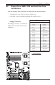
JBT1
DIMM2A
SP1
JI2C1
JI2C2
JL1
LED5
LED6
LED3
JWD1
JPG1
JPL2
JPA1
Fan 4
JD1
LED4
JWOL1
JPWF1
JAR
8-Pin PWR
I-Button
LAN
CTRL
VGA
CTRL
S I/O
SATA4
SATA3
SATA2
SATA1
SATA0
SATA5
SATA-GPIO0
Battery
SAS0
SAS1
SAS2
SAS3
SAS4
SAS5
SAS6
SAS7
PWR LED
JP1
JP2
COM2
JWOR1
JKEY1
Buzzer
BIOS
SATA-GPIO1
ITE
CTRL
LAN
CTRL
DIMM1A
DIMM2B
DIMM1B
DIMM2C
DIMM1C
LED1
SAS-GPIO0
SAS-GPIO1
24-Pin PWR
JPA2
System Status LED
Fan 1
CPU1 VRM OH LED
CPU2 VRM OH LED
Floppy
IDE
BPI
2
C
USB2/3
SMB_PS
KB/MS
COM1
VGA
FAN6
Slot4 PCI-E x4(in x8 slot)
Slot1 PCI 33MHz
SIMLC
USB0/1
LAN1
LAN2
FAN5
CPU1
CPU2
Fan 2
Fan 3
FP CTRL
USB4/5
Slot2 PCI 33MHz
Slot3 PCI 33MHz
Slot5 PCI-E x8
Slot6 PCI-E x8
Intel
5100
North Bridge
South Bridge
ICH9R
Intel
LSI
SAS
CTRL
JPL1
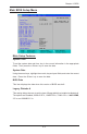
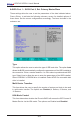
X7DCL-3/i
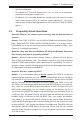
2-8 Floppy Drive, SIMLC IPMI and Hard Disk Drive
Connections
Note the following when connecting the oppy and hard disk drive cables:
• The oppy disk drive cable has seven twisted wires.
• A red mark on a wire typically designates the location of pin 1.
A
A. Floppy Disk Drive
Floppy Connector
The oppy connector is located at
JFDD1. See the table below for pin
denitions.
Floppy Drive Connector
PinDenitions(Floppy)
Pin# Denition Pin # Denition
1 Ground 2 FDHDIN
3 Ground 4 Reserved
5 Key 6 FDEDIN
7 Ground 8 Index
9 Ground 10 Motor Enable
11 Ground 12 Drive Select B
13 Ground 14 Drive Select B
15 Ground 16 Motor Enable
17 Ground 18 DIR
19 Ground 20 STEP
21 Ground 22 Write Data
23 Ground 24 Write Gate
25 Ground 26 Track 00
27 Ground 28 Write Protect
29 Ground 30 Read Data
31 Ground 32 Side 1 Select
33 Ground 34 Diskette