
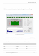
Application Guide


0.15mm
0.18mm
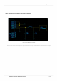
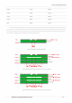
If it is a 2-layer board, the signal layer is the Top layer, and the reference ground is the Bottom layer, as shown in Figure 3 below. If it is a 4-layer board, the reference ground can be the 2nd
Figure 4: Schematic diagram of the four-layer board LAYOUT (the reference ground is the third layer)
Figure 5: Schematic diagram of the four-layer board LAYOUT (the reference ground is the fourth layer)
1.0mm
2mm
Sunivision Technology Development Co.,Ltd
0.8mm
7 / 9
1.6mm
0.8mm
0.8mm
It is 5 times the width of the signal line, as shown in Figure 5 below. If it is more than 6-layer board and so on.
Figure 3: Schematic diagram of two-layer board LAYOUT
Layer, Layer 3 or Layer 4. If the reference ground is the third layer, the second layer directly under the signal layer should be forbidden, and the width of the forbidden area should be at least the signal line.
0.8mm
RF LAYOUT Application Guide
0.16mm
0.8mm 0.17mm
0.8mm
5 times the width, as shown in Figure 4 below. If the reference ground is the 4th layer, the 2nd and 3rd layers directly under the signal layer must be forbidden to be laid, and the width of the forbidden area shall be at least
0.14mm
1.2mm