
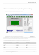
Application Guide

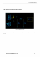
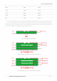

Among them, C1, R1, and C2 are reserved matching circuits to optimize the performance of the antenna port. The default values are: R1 is pasted with 0R resistor; C1 is not pasted;
C2 is not pasted.
5 / 9
Sunivision Technology Development Co.,Ltd
Figure 1: Module RF Reference Schematic
RF LAYOUT Application Guide
2 RF Interface Schematic Recommendations