
Application Guide


Sunivision Technology Development Co.,Ltd
3 / 9
RF LAYOUT Application Guide
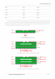
image index
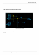
Figure 2: Schematic diagram of coplanar waveguide structure ................................................ ...................................................... ............................................... 7
Figure 4: Schematic diagram of four-layer board LAYOUT (the reference ground is the third layer)................................. ...................................................... ......... 8
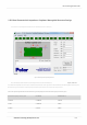
Figure 6: Example diagram of PCB LAYOUT................................................ ...................................................... ......................................... 9
Figure 5: Schematic diagram of four-layer board LAYOUT (the reference ground is the fourth layer)................................. ...................................................... ......... 8
Figure 3: Schematic diagram of two-layer board LAYOUT................................................ ...................................................... ....................................... 8
Figure 1: Module RF Reference Schematic ............................................... ...................................................... ............................................... 6