
User Manual


91
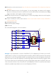
MR: Reset pin, active at low lev el; here it is directly connected to 5V to keep the chip from
resetting.
SH_CP: Time sequence input of shift register. On the rising edge, the data in shift register
moves successively one bit, i.e. data in Q1 mov es to Q2, and so forth. While on the falling
edge, the data in shift register remain unchanged.
ST_CP: Time sequence input of storage register. On the rising edge, data in the shift register
moves into memory register.
OE: Output enable pin, activ e at low level; here connected to GND to keep 74HC595 in
output enable state.
DS: Serial data input pin
VCC: Positive supply voltage
GND: Ground
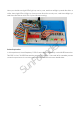
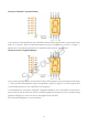
The schematic diagram is shown as below:
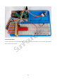
Principle: In this experiment, connect 74HC595’s ST_CP to Raspberry Pi’s B18, SH_CP to B27,
and DS to B17; connect a current-limit resistor and then a LED to Q0-Q7 respectiv ely; connect
MR and VCC to 5V, CE and GND to GND. I nput data in DS pin to the shift register when SH_CP
(the clock input of the shift register) is at the rising edge, and to the memory register when
ST_CP (the clock input of the memory) is at the rising edge, and output to Q0-Q7. Then you
can control the states of SH_CP and ST_CP via Raspberry Pi GPIO to transform serial input
data into parallel output data so as to save Raspberry Pi GPIOs.
SunFounder