
Data Sheet

1997 Apr 02 15
Philips Semiconductors Product specification
Remote 8-bit I/O expander for I
2
C-bus
PCF8574
11 I
2
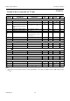
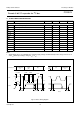
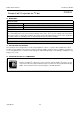
C-BUS TIMING CHARACTERISTICS
Note
1. All the timing values are valid within the operating supply voltage and ambient temperature range and refer to V
IL
and V
IH
with an input voltage swing of V
SS
to V
DD
.
SYMBOL PARAMETER MIN. TYP. MAX. UNIT
I
2
C-BUS TIMING (see Fig.15; note 1)
f
SCL
SCL clock frequency −−100 kHz
t
SW
tolerable spike width on bus −−100 ns
t
BUF
bus free time 4.7 −−µs
t
SU;STA
START condition set-up time 4.7 −−µs
t
HD;STA
START condition hold time 4.0 −−µs
t
LOW
SCL LOW time 4.7 −−µs
t
HIGH
SCL HIGH time 4.0 −−µs
t
r
SCL and SDA rise time −−1.0 µs
t
f
SCL and SDA fall time −−0.3 µs
t
SU;DAT
data set-up time 250 −−ns
t
HD;DAT
data hold time 0 −−ns
t
VD;DAT
SCL LOW to data out valid −−3.4 µs
t
SU;STO
STOP condition set-up time 4.0 −−µs
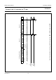
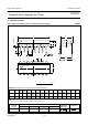
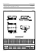
Fig.15 I
2
C-bus timing diagram.
handbook, full pagewidth
PROTOCOL
SCL
SDA
MBD820
BIT 0
LSB
(R/W)
t
HD;STA
t
SU;DAT
t
HD;DAT
t
VD;DAT
t
SU;STO
t
f
r
t
t
BUF
t
SU;STA
t
LOW
t
HIGH
1 / f
SCL
START
CONDITION
(S)
BIT 7
MSB
(A7)
BIT 6
(A6)
ACKNOWLEDGE
(A)
STOP
CONDITION
(P)