
Data Sheet

1997 Apr 02 14
Philips Semiconductors Product specification
Remote 8-bit I/O expander for I
2
C-bus
PCF8574
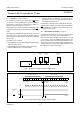
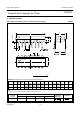
Note
1. The Power-on reset circuit resets the I
2
C-bus logic with V
DD
<V
POR
and sets all I/Os to logic 1 (with current source
to V
DD
).
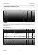
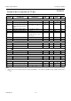
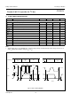
I/Os
V
IL
LOW level input voltage −0.5 − +0.3V
DD
V
V
IH
HIGH level input voltage 0.7V
DD
− V
DD
+ 0.5 V
I
IHL(max)
maximum allowed input
current through protection
diode
V
I
≥ V
DD
or V
I
≤ V
SS
−−±400 µA
I
OL
LOW level output current V
OL
=1V; V
DD
=5V 10 25 − mA
I
OH
HIGH level output current V
OH
=V
SS
30 − 300 µA
I
OHt
transient pull-up current HIGH during acknowledge
(see Fig.14); V
OH
=V
SS
;
V
DD
= 2.5 V
−−1−mA
C
i
input capacitance −−10 pF
C
o
output capacitance −−10 pF
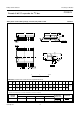
Port timing; C
L
≤ 100 pF (see Figs 10 and 11)
t
pv
output data valid −−4µs
t
su
input data set-up time 0 −− µs
t
h
input data hold time 4 −− µs
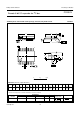
Interrupt
INT (see Fig.13)
I
OL
LOW level output current V
OL
= 0.4 V 1.6 −− mA
I
L
leakage current V
I
=V
DD
or V
SS
−1 − +1 µA
TIMING;C
L
≤100 PF
t
iv
input data valid time −−4µs
t
ir
reset delay time −−4µs
Select inputs A0 to A2
V
IL
LOW level input voltage −0.5 − +0.3V
DD
V
V
IH
HIGH level input voltage 0.7V
DD
− V
DD
+ 0.5 V
I
LI
input leakage current pin at V
DD
or V
SS
−250 − +250 nA
SYMBOL PARAMETER CONDITIONS MIN. TYP. MAX. UNIT