
Data Sheet

1997 Apr 02 13
Philips Semiconductors Product specification
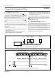
Remote 8-bit I/O expander for I
2
C-bus
PCF8574
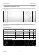
8 LIMITING VALUES
In accordance with the Absolute Maximum Rating System (IEC 134).
9 HANDLING
Inputs and outputs are protected against electrostatic discharge in normal handling. However, to be totally safe, it is
desirable to take precautions appropriate to handling MOS devices. Advice can be found in Data Handbook IC12 under
“Handling MOS Devices”
.
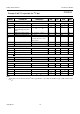
10 DC CHARACTERISTICS
V
DD
= 2.5 to 6 V; V
SS
= 0 V; T
amb
= −40 to +85 °C; unless otherwise specified.
SYMBOL PARAMETER MIN. MAX. UNIT
V
DD
supply voltage −0.5 +7.0 V
V
I
input voltage V
SS
− 0.5 V
DD
+ 0.5 V
I
I
DC input current −±20 mA
I
O
DC output current −±25 mA
I
DD
supply current −±100 mA
I
SS
supply current −±100 mA
P
tot
total power dissipation − 400 mW
P
O
power dissipation per output − 100 mW
T
stg
storage temperature −65 +150 °C
T
amb
operating ambient temperature −40 +85 °C
SYMBOL PARAMETER CONDITIONS MIN. TYP. MAX. UNIT
Supply
V
DD
supply voltage 2.5 − 6.0 V
I
DD
supply current operating mode; V
DD
=6V;
no load; V
I
=V
DD
or V
SS
;
f
SCL
= 100 kHz
− 40 100 µA
I
stb
standby current standby mode; V
DD
=6V;
no load; V
I
=V
DD
or V
SS
− 2.5 10 µA
V
POR
Power-on reset voltage V
DD
= 6 V; no load;
V
I
=V
DD
or V
SS
; note 1
− 1.3 2.4 V
Input SCL; input/output SDA
V
IL
LOW level input voltage −0.5 − +0.3V
DD
V
V
IH
HIGH level input voltage 0.7V
DD
− V
DD
+ 0.5 V
I
OL
LOW level output current V
OL
= 0.4 V 3 −− mA
I
L
leakage current V
I
=V
DD
or V
SS
−1 − +1 µA
C
i
input capacitance V
I
=V
SS
−−7pF