
Data Sheet

DS18B20
2 of 27
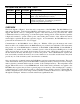
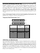
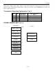
DETAILED PIN DESCRIPTION Table 1
PIN
8PIN SOIC
PIN
TO92 SYMBOL DESCRIPTION
5 1 GND Ground.
42DQData Input/Output pin. For 1-Wire operation: Open
drain. (See “Parasite Power” section.)
33V
DD
Optional V
DD
pin. See “Parasite Power” section for
details of connection. V
DD
must be grounded for
operation in parasite power mode.
DS18B20Z (8-pin SOIC): All pins not specified in this table are not to be connected.
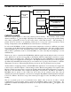
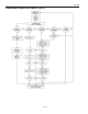
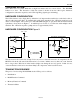
OVERVIEW
The block diagram of Figure 1 shows the major components of the DS18B20. The DS18B20 has four
main data components: 1) 64-bit lasered ROM, 2) temperature sensor, 3) nonvolatile temperature alarm
triggers TH and TL, and 4) a configuration register. The device derives its power from the 1-Wire
communication line by storing energy on an internal capacitor during periods of time when the signal line
is high and continues to operate off this power source during the low times of the 1-Wire line until it
returns high to replenish the parasite (capacitor) supply. As an alternative, the DS18B20 may also be
powered from an external 3 volt - 5.5 volt supply.
Communication to the DS18B20 is via a 1-Wire port. With the 1-Wire port, the memory and control
functions will not be available before the ROM function protocol has been established. The master must
first provide one of five ROM function commands: 1) Read ROM, 2) Match ROM, 3) Search ROM, 4)
Skip ROM, or 5) Alarm Search. These commands operate on the 64-bit lasered ROM portion of each
device and can single out a specific device if many are present on the 1-Wire line as well as indicate to
the bus master how many and what types of devices are present. After a ROM function sequence has
been successfully executed, the memory and control functions are accessible and the master may then
provide any one of the six memory and control function commands.
One control function command instructs the DS18B20 to perform a temperature measurement. The result
of this measurement will be placed in the DS18B20’s scratch-pad memory, and may be read by issuing a
memory function command which reads the contents of the scratchpad memory. The temperature alarm
triggers TH and TL consist of 1 byte EEPROM each. If the alarm search command is not applied to the
DS18B20, these registers may be used as general purpose user memory. The scratchpad also contains a
configuration byte to set the desired resolution of the temperature to digital conversion. Writing TH, TL,
and the configuration byte is done using a memory function command. Read access to these registers is
through the scratchpad. All data is read and written least significant bit first.