
Data Sheet

PCF8563_5 © NXP B.V. 2007. All rights reserved.
Product data sheet Rev. 05 — 17 July 2007 6 of 32
NXP Semiconductors
PCF8563
Real time clock/calendar
7.6 Register organization
7.6.1 Control/status 1 register
7.6.2 Control/status 2 register
Bits TF and AF: When an alarm occurs, AF is set to logic 1. Similarly, at the end of a timer
countdown, TF is set to logic 1. These bits maintain their value until overwritten by
software. If both timer and alarm interrupts are required in the application, the source of
the interrupt can be determined by reading these bits. To prevent one flag being
overwritten while clearing another a logic AND is performed during a write access.
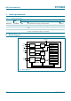
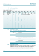
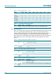
Table 3. Formatted registers overview
Bit positions labelled as x are not implemented. Bit positions labelled with 0 should always be written with logic 0; if read they
could be either logic 0 or logic 1.
Address Register name Bit 7 Bit 6 Bit 5 Bit 4 Bit 3 Bit 2 Bit 1 Bit 0
00h control/status 1 TEST1 0 STOP 0 TESTC 0 0 0
01h control/status 2 0 0 0 TI/TP AF TF AIE TIE
02h seconds VL <seconds 00 to 59 coded in BCD>
03h minutes x <minutes 00 to 59 coded in BCD>
04h hours x x <hours 00 to 23 coded in BCD>
05h days x x <days 01 to 31 coded in BCD>
06h weekdays xxxxx <weekdays 0 to 6>
07h months/century C x x <months 01 to 12 coded in BCD>
08h years <years 00 to 99 coded in BCD>
09h minute alarm AE <minute alarm 00 to 59 coded in BCD>
0Ah hour alarm AE x <hour alarm 00 to 23 coded in BCD>
0Bh day alarm AE x <day alarm 01 to 31 coded in BCD>
0Ch weekday alarm AE xxxx<weekday alarm 0 to 6>
0Dh CLKOUT control FE xxxxxFD1FD0
0Eh timer control AT xxxxxTD1TD0
0Fh timer <timer countdown value>
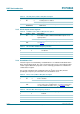
Table 4. Control/status 1 (address 00h) bits description
Bit Symbol Value Description
7 TEST1 0 normal mode
1 EXT_CLK test mode
6 0 default value is logic 0
5 STOP 0 RTC source clock runs
1 all RTC divider chain flip-flops are asynchronously set to logic 0;
the RTC clock is stopped (CLKOUT at 32.768 kHz is still
available)
4 0 default value is logic 0
3 TESTC 0 Power-on reset override facility is disabled; set to logic 0 for
normal operation
1 Power-on reset override may be enabled
2 to 0 0 default value is logic 0