
Data Sheet

PCF8563_5 © NXP B.V. 2007. All rights reserved.
Product data sheet Rev. 05 — 17 July 2007 5 of 32
NXP Semiconductors
PCF8563
Real time clock/calendar
7.2 Timer
The 8-bit countdown timer at address 0Fh is controlled by the timer control register at
address 0Eh. The timer control register determines one of 4 source clock frequencies for
the timer (4096 Hz, 64 Hz, 1 Hz, or
1
⁄
60
Hz), and enables or disables the timer. The timer
counts down from a software-loaded 8-bit binary value. At the end of every countdown,
the timer sets the Timer Flag (TF). The TF may only be cleared by software. The
asserted TF can be used to generate an interrupt (INT). The interrupt may be generated
as a pulsed signal every countdown period or as a permanently active signal which
follows the condition of TF. Bit TI/TP is used to control this mode selection. When reading
the timer, the current countdown value is returned.
7.3 Clock output
A programmable square wave is available at pin CLKOUT. Operation is controlled by the
CLKOUT control register at address 0Dh. Frequencies of 32.768 kHz (default), 1024 Hz,
32 Hz and 1 Hz can be generated for use as a system clock, microcontroller clock, input to
a charge pump, or for calibration of the oscillator. CLKOUT is an open-drain output and
enabled at power-on. If disabled it becomes high-impedance.
7.4 Reset
The PCF8563 includes an internal reset circuit which is active whenever the oscillator is
stopped. In the reset state the I
2
C-bus logic is initialized and all registers are reset
according to Table 25.
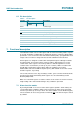
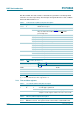
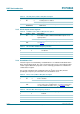
7.5 Voltage-low detector
The PCF8563 has an on-chip voltage-low detector (see Figure 7). When V
DD
drops below
V
low
, bit VL in the seconds register is set to indicate that the integrity of the clock
information is no longer guaranteed. The VL flag can only be cleared by software.
Bit VL is intended to detect the situation when V
DD
is decreasing slowly, for example under
battery operation. Should V
DD
reach V
low
before power is re-asserted then bit VL is set.
This will indicate that the time may be corrupted.
Fig 7. Voltage-low detection
VL set
normal power
operation
period of battery
operation
t
V
DD
V
low
mgr887