
Data Sheet

PCF8563_5 © NXP B.V. 2007. All rights reserved.
Product data sheet Rev. 05 — 17 July 2007 4 of 32
NXP Semiconductors
PCF8563
Real time clock/calendar
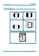
6.2 Pin description
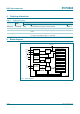
7. Functional description
The PCF8563 contains sixteen 8-bit registers with an auto-incrementing address register,
an on-chip 32.768 kHz oscillator with one integrated capacitor, a frequency divider which
provides the source clock for the Real Time Clock/calender (RTC), a programmable clock
output, a timer, an alarm, a voltage-low detector and a 400 kHz I
2
C-bus interface.
All 16 registers are designed as addressable 8-bit parallel registers although not all bits
are implemented. The first two registers (memory address 00h and 01h) are used as
control and/or status registers. The memory addresses 02h through 08h are used as
counters for the clock function (seconds up to years counters). Address locations 09h
through 0Ch contain alarm registers which define the conditions for an alarm.
Address 0Dh controls the CLKOUT output frequency. 0Eh and 0Fh are the timer control
and timer registers, respectively.
The seconds, minutes, hours, days, weekdays, months, years as well as the minute alarm,
hour alarm, day alarm and weekday alarm registers are all coded in Binary Coded
Decimal (BCD) format.
When one of the RTC registers is read the contents of all counters are frozen. Therefore,
faulty reading of the clock/calendar during a carry condition is prevented.
7.1 Alarm function modes
By clearing the MSB of one or more of the alarm registers (bit AE = alarm enable), the
corresponding alarm condition(s) will be active. In this way an alarm can be generated
from once per minute up to once per week. The alarm condition sets the Alarm Flag (AF).
The asserted AF can be used to generate an interrupt (INT). The AF can only be cleared
by software.
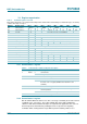
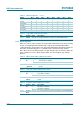
Table 2. Pin description
Symbol Pin Description
DIP8, SO8,
TSSOP8
HVSON10
OSCI 1 1 oscillator input
OSCO 2 2 oscillator output
n.c - 3 not connected
INT 3 4 interrupt output (open-drain; active LOW)
V
SS
4 5 ground
SDA 5 6 serial data input and output
SCL 6 7 serial clock input
CLKOUT 7 8 clock output, open-drain
V
DD
8 9 positive supply voltage
n.c - 10 not connected