
Data Sheet


NXP Semiconductors
PCF8563
Real time clock/calendar
© NXP B.V. 2007. All rights reserved.
For more information, please visit: http://www.nxp.com
For sales office addresses, please send an email to: salesaddresses@nxp.com
Date of release: 17 July 2007
Document identifier: PCF8563_5
Please be aware that important notices concerning this document and the product(s)
described herein, have been included in section ‘Legal information’.
19. Contents
1 General description . . . . . . . . . . . . . . . . . . . . . . 1
2 Features . . . . . . . . . . . . . . . . . . . . . . . . . . . . . . . 1
3 Applications . . . . . . . . . . . . . . . . . . . . . . . . . . . . 1
4 Ordering information. . . . . . . . . . . . . . . . . . . . . 2
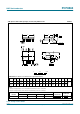
5 Block diagram . . . . . . . . . . . . . . . . . . . . . . . . . . 2
6 Pinning information. . . . . . . . . . . . . . . . . . . . . . 3
6.1 Pinning . . . . . . . . . . . . . . . . . . . . . . . . . . . . . . . 3
6.2 Pin description . . . . . . . . . . . . . . . . . . . . . . . . . 4
7 Functional description . . . . . . . . . . . . . . . . . . . 4
7.1 Alarm function modes. . . . . . . . . . . . . . . . . . . . 4
7.2 Timer. . . . . . . . . . . . . . . . . . . . . . . . . . . . . . . . . 5
7.3 Clock output . . . . . . . . . . . . . . . . . . . . . . . . . . . 5
7.4 Reset . . . . . . . . . . . . . . . . . . . . . . . . . . . . . . . . 5
7.5 Voltage-low detector . . . . . . . . . . . . . . . . . . . . . 5
7.6 Register organization . . . . . . . . . . . . . . . . . . . . 6
7.6.1 Control/status 1 register . . . . . . . . . . . . . . . . . . 6
7.6.2 Control/status 2 register . . . . . . . . . . . . . . . . . . 6
7.6.3 Time and date registers . . . . . . . . . . . . . . . . . . 7
7.6.4 Alarm registers . . . . . . . . . . . . . . . . . . . . . . . . . 9
7.6.5 Clock output control register. . . . . . . . . . . . . . 10
7.6.6 Countdown timer. . . . . . . . . . . . . . . . . . . . . . . 10
7.7 EXT_CLK test mode. . . . . . . . . . . . . . . . . . . . 11
7.8 Power-On Reset (POR) override . . . . . . . . . . 11
8 Characteristics of the I
2
C-bus. . . . . . . . . . . . . 12
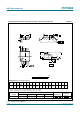
8.1 Bit transfer . . . . . . . . . . . . . . . . . . . . . . . . . . . 13
8.2 Start and stop conditions . . . . . . . . . . . . . . . . 13
8.3 System configuration . . . . . . . . . . . . . . . . . . . 13
8.4 Acknowledge . . . . . . . . . . . . . . . . . . . . . . . . . 14
8.5 I
2
C-bus protocol . . . . . . . . . . . . . . . . . . . . . . . 14
8.5.1 Addressing . . . . . . . . . . . . . . . . . . . . . . . . . . . 14
8.5.2 Clock/calendar read/write cycles . . . . . . . . . . 15
9 Limiting values. . . . . . . . . . . . . . . . . . . . . . . . . 16
10 Static characteristics. . . . . . . . . . . . . . . . . . . . 16
11 Dynamic characteristics . . . . . . . . . . . . . . . . . 19
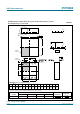
12 Application information. . . . . . . . . . . . . . . . . . 20
12.1 Quartz frequency adjustment . . . . . . . . . . . . . 21
12.1.1 Method 1: fixed OSCI capacitor . . . . . . . . . . . 21
12.1.2 Method 2: OSCI trimmer. . . . . . . . . . . . . . . . . 21
12.1.3 Method 3: OSCO output . . . . . . . . . . . . . . . . . 21
13 Package outline . . . . . . . . . . . . . . . . . . . . . . . . 22
14 Handling information. . . . . . . . . . . . . . . . . . . . 26
15 Soldering . . . . . . . . . . . . . . . . . . . . . . . . . . . . . 26
15.1 Introduction to soldering . . . . . . . . . . . . . . . . . 26
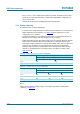
15.2 Wave and reflow soldering . . . . . . . . . . . . . . . 26
15.3 Wave soldering . . . . . . . . . . . . . . . . . . . . . . . . 26
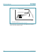
15.4 Reflow soldering. . . . . . . . . . . . . . . . . . . . . . . 27
16 Revision history . . . . . . . . . . . . . . . . . . . . . . . 29
17 Legal information . . . . . . . . . . . . . . . . . . . . . . 30
17.1 Data sheet status . . . . . . . . . . . . . . . . . . . . . . 30
17.2 Definitions . . . . . . . . . . . . . . . . . . . . . . . . . . . 30
17.3 Disclaimers. . . . . . . . . . . . . . . . . . . . . . . . . . . 30
17.4 Trademarks . . . . . . . . . . . . . . . . . . . . . . . . . . 30
18 Contact information . . . . . . . . . . . . . . . . . . . . 30
19 Contents. . . . . . . . . . . . . . . . . . . . . . . . . . . . . . 32