
Data Sheet

PCF8563_5 © NXP B.V. 2007. All rights reserved.
Product data sheet Rev. 05 — 17 July 2007 19 of 32
NXP Semiconductors
PCF8563
Real time clock/calendar
11. Dynamic characteristics
[1] Unspecified for f
CLKOUT
= 32.768 kHz.
[2] All timing values are valid within the operating supply voltage at ambient temperature and referenced to V
IL
and V
IH
with an input voltage
swing of V
SS
to V
DD
.
[3] A detailed description of the I
2
C-bus specification, with applications, is given in brochure
The I
2
C-bus and how to use it
. This brochure
may be ordered using the code 9398 393 40011.
[4] I
2
C-bus access time between two STARTs or between a START and a STOP condition to this device must be less than one second.
Table 28. Dynamic characteristics
V
DD
= 1.8 V to 5.5 V; V
SS
=0V; T
amb
=
−
40
°
C to +85
°
C; f
osc
= 32.768 kHz; quartz R
s
=40k
Ω
; C
L
= 8 pF; unless otherwise
specified.
Symbol Parameter Conditions Min Typ Max Unit
Oscillator
C
L(itg)
integrated load
capacitance
15 25 35 pF
∆f
osc
/f
osc
relative oscillator
frequency variation
∆V
DD
= 200 mV;
T
amb
=25°C
-2× 10
-7
--
Quartz crystal parameters (f = 32.768 kHz)
R
s
series resistance - - 40 kΩ
C
L
parallel load capacitance - 10 - pF
C
trim
trimmer capacitance 5 - 25 pF
CLKOUT output
δ
CLKOUT
CLKOUT duty cycle
[1]
-50-%
I
2
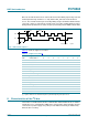
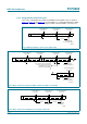
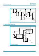
C-bus timing characteristics (see Figure 21)
[2][3]
f
SCL
SCL clock frequency
[4]
- - 400 kHz
t
HD;STA
hold time (repeated)
START condition
0.6 - - µs
t
SU;STA
set-up time for a repeated
START condition
0.6 - - µs
t
LOW
LOW period of the SCL
clock
1.3 - - µs
t
HIGH
HIGH period of the SCL
clock
0.6 - - µs
t
r
rise time of both SDA and
SCL signals
SDA - - 0.3 µs
SCL - - 0.3 µs
t
f
fall time of both SDA and
SCL signals
SDA - - 0.3 µs
SCL - - 0.3 µs
C
b
capacitive bus line load - - 400 pF
t
SU;DAT
data set-up time 100 - - ns
t
HD;DAT
data hold time 0 - - ns
t
SU;STO
set-up time for STOP
condition
0.6 - - µs
t
w(spike)
tolerable spike width on
bus
--50ns