
Data Sheet

PCF8563_5 © NXP B.V. 2007. All rights reserved.
Product data sheet Rev. 05 — 17 July 2007 16 of 32
NXP Semiconductors
PCF8563
Real time clock/calendar
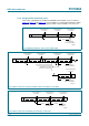
9. Limiting values
10. Static characteristics
Table 26. Limiting values
In accordance with the Absolute Maximum Rating System (IEC 60134)
Symbol Parameter Min Max Unit
V
DD
supply voltage −0.5 +6.5 V
I
DD
supply current −50 +50 mA
V
I
input voltage on pins SCL and SDA −0.5 +6.5 V
input voltage on pin OSCI −0.5 V
DD
+ 0.5 V
V
O
output voltage on pins CLOCKOUT
and
INT
−0.5 +6.5 V
I
I
DC input current at any input −10 +10 mA
I
O
DC output current at any output −10 +10 mA
P
tot
total power dissipation - 300 mW
T
amb
ambient temperature −40 +85 °C
T
stg
storage temperature −65 +150 °C
Table 27. Static characteristics
V
DD
= 1.8 V to 5.5 V; V
SS
=0V; T
amb
=
−
40
°
C to +85
°
C; f
osc
= 32.768 kHz; quartz R
s
=40k
Ω
; C
L
= 8 pF; unless otherwise
specified.
Symbol Parameter Conditions Min Typ Max Unit
Supplies
V
DD
supply voltage interface inactive; f
SCL
= 0 Hz;
T
amb
=25°C; see Figure 20
[1]
1.0 - 5.5 V
interface active;
f
SCL
= 400 kHz; see Figure 20
[1]
1.8 - 5.5 V
clock data integrity;
T
amb
=25°C
V
low
- 5.5 V
I
DD1
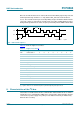
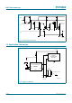
supply current 1 interface active; see Figure 19
f
SCL
= 400 kHz - - 800 µA
f
SCL
= 100 kHz - - 200 µA
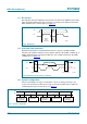
I
DD2
supply current 2 interface inactive (f
SCL
= 0 Hz);
CLKOUT disabled;
T
amb
=25°C; see Figure 17
[2]
V
DD
= 5.0 V - 275 550 nA
V
DD
= 3.0 V - 250 500 nA
V
DD
= 2.0 V - 225 450 nA
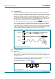
interface inactive (f
SCL
= 0 Hz);
CLKOUT disabled;
T
amb
= −40 °C to +85 °C;
see
Figure 17
[2]
V
DD
= 5.0 V - 500 750 nA
V
DD
= 3.0 V - 400 650 nA
V
DD
= 2.0 V - 400 600 nA