
Data Sheet

PCF8563_5 © NXP B.V. 2007. All rights reserved.
Product data sheet Rev. 05 — 17 July 2007 14 of 32
NXP Semiconductors
PCF8563
Real time clock/calendar
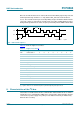
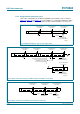
8.4 Acknowledge
The number of data bytes transferred between the START and STOP conditions from
transmitter to receiver is unlimited. Each byte of eight bits is followed by an acknowledge
bit. The acknowledge bit is a HIGH-level signal put on the bus by the transmitter during
which time the master generates an extra acknowledge related clock pulse. A slave
receiver which is addressed must generate an acknowledge after the reception of each
byte. Also a master receiver must generate an acknowledge after the reception of each
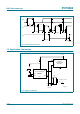
byte that has been clocked out of the slave transmitter (see Figure 12).
The device that acknowledges must pull down the SDA line during the acknowledge clock
pulse, so that the SDA line is stable LOW during the HIGH period of the acknowledge
related clock pulse (set-up and hold times must be taken into consideration). A master
receiver must signal an end of data to the transmitter by not generating an acknowledge
on the last byte that has been clocked out of the slave. In this event the transmitter must
leave the data line HIGH to enable the master to generate a stop condition.
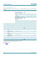
8.5 I
2
C-bus protocol
8.5.1 Addressing
Before any data is transmitted on the I
2
C-bus, the device which should respond is
addressed first. The addressing is always carried out with the first byte transmitted after
the start procedure.
The PCF8563 acts as a slave receiver or slave transmitter. Therefore the clock signal SCL
is only an input signal, but the data signal SDA is a bidirectional line.
The PCF8563 slave address is shown in Figure 13.
Fig 12. Acknowledgement on the I
2
C-bus
mbc602
S
START
condition
9821
clock pulse for
acknowledgement
not acknowledge
acknowledge
data output
by transmitter
data output
by receiver
SCL from
master
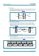
Fig 13. Slave address
mce189
1 0 1 0 0 0 1 R/W
group 1
group 2