
Data Sheet

PCF8563_5 © NXP B.V. 2007. All rights reserved.
Product data sheet Rev. 05 — 17 July 2007 13 of 32
NXP Semiconductors
PCF8563
Real time clock/calendar
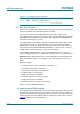
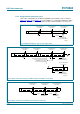
8.1 Bit transfer
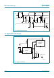
One data bit is transferred during each clock pulse. The data on the SDA line must remain
stable during the HIGH period of the clock pulse as changes in the data line at this time
will be interpreted as a control signal (see Figure 9).
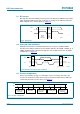
8.2 Start and stop conditions
Both data and clock lines remain HIGH when the bus is not busy. A HIGH-to-LOW
transition of the data line, while the clock is HIGH is defined as the START condition (S). A
LOW-to-HIGH transition of the data line while the clock is HIGH is defined as the STOP
condition (P); see Figure 10.
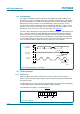
8.3 System configuration
A device generating a message is a transmitter, a device receiving a message is the
receiver. The device that controls the message is the master and the devices which are
controlled by the master are the slaves (see Figure 11).
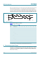
Fig 9. Bit transfer
mbc621
data line
stable;
data valid
change
of data
allowed
SDA
SCL
Fig 10. Definition of start and stop conditions
mbc622
SDA
SCL
P
STOP condition
SDA
SCL
S
START condition
Fig 11. System configuration
mba605
MASTER
TRANSMITTER /
RECEIVER
SLAVE
RECEIVER
SLAVE
TRANSMITTER /
RECEIVER
MASTER
TRANSMITTER
MASTER
TRANSMITTER /
RECEIVER
SDA
SCL