
Data Sheet

PCF8563_5 © NXP B.V. 2007. All rights reserved.
Product data sheet Rev. 05 — 17 July 2007 12 of 32
NXP Semiconductors
PCF8563
Real time clock/calendar
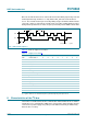
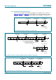
Once the override mode has been entered, the device immediately stops being reset and
normal operation may commence i.e. entry into the EXT_CLK test mode via I
2
C-bus
access. The override mode may be cleared by writing a logic 0 to TESTC. TESTC must be
set to logic 1 before re-entry into the override mode is possible. Setting TESTC to logic 0
during normal operation has no effect except to prevent entry into the POR override mode.
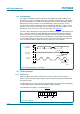
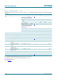
Table 25 shows the register reset values.
[1] registers marked ‘x’ are undefined at power-up and unchanged by subsequent resets.
8. Characteristics of the I
2
C-bus
The I
2
C-bus is for bidirectional, two-line communication between different ICs or modules.
The two lines are a serial data line (SDA) and a serial clock line (SCL). Both lines must be
connected to a positive supply via a pull-up resistor. Data transfer may be initiated only
when the bus is not busy.
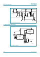
Fig 8. POR override sequence
mgm664
SCL
500 ns 2000 ns
SDA
8 ms
override active
power up
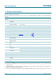
Table 25: Register reset value
[1]
Address Register name Bit 7 Bit 6 Bit 5 Bit 4 Bit 3 Bit 2 Bit 1 Bit 0
00h control/status 1 0 0 0 0 1 0 0 0
01h control/status 2 x x 0 0 0 0 0 0
02h seconds 1 x x x x x x x
03h minutes 1 x x x x x x x
04h hours x x x x x x x x
05hdays xxxxxxxx
06h weekdays x x x x x x x x
07h months/century x x x x x x x x
08h years x x x x x x x x
09h minute alarm 1 x x x x x x x
0Ah hour alarm 1 x x x x x x x
0Bh day alarm 1 x x x x x x x
0Ch weekday alarm 1 x x x x x x x
0Dh CLKOUT control 1 x x x x x 0 0
0Eh timer control 0 x x x x x 1 1
0Fh timer x x x x x x x x