
Data Sheet

PCF8563_5 © NXP B.V. 2007. All rights reserved.
Product data sheet Rev. 05 — 17 July 2007 11 of 32
NXP Semiconductors
PCF8563
Real time clock/calendar
7.7 EXT_CLK test mode
A test mode is available which allows for on-board testing. In such a mode it is possible to
set up test conditions and control the operation of the RTC.
The test mode is entered by setting bit TEST1 in control/status1 register. Then
pin CLKOUT becomes an input. The test mode replaces the internal 64 Hz signal with the
signal applied to pin CLKOUT. Every 64 positive edges applied to pin CLKOUT will then
generate an increment of one second.
The signal applied to pin CLKOUT should have a minimum pulse width of 300 ns and a
minimum period of 1000 ns. The internal 64 Hz clock, now sourced from CLKOUT, is
divided down to 1 Hz by a 2
6
divide chain called a pre-scaler. The pre-scaler can be set
into a known state by using bit STOP. When bit STOP is set, the pre-scaler is reset to 0
(STOP must be cleared before the pre-scaler can operate again).
From a STOP condition, the first 1 second increment will take place after 32 positive
edges on CLKOUT. Thereafter, every 64 positive edges will cause a 1 second increment.
Remark: Entry into EXT_CLK test mode is not synchronized to the internal 64 Hz clock.
When entering the test mode, no assumption as to the state of the pre-scaler can be
made.
Operation example:
1. Set EXT_CLK test mode (control/status 1, bit TEST1 = 1)
2. Set STOP (control/status 1, bit STOP = 1)
3. Clear STOP (control/status 1, bit STOP = 0)
4. Set time registers to desired value
5. Apply 32 clock pulses to CLKOUT
6. Read time registers to see the first change
7. Apply 64 clock pulses to CLKOUT
8. Read time registers to see the second change
Repeat 7 and 8 for additional increments.
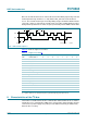
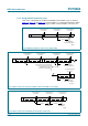
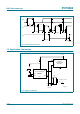
7.8 Power-On Reset (POR) override
The POR duration is directly related to the crystal oscillator start-up time. Due to the long
start-up times experienced by these types of circuits, a mechanism has been built in to
disable the POR and hence speed up on-board test of the device. The setting of this mode
requires that the I
2
C-bus pins, SDA and SCL, be toggled in a specific order as shown in
Figure 8. All timings are required minimums.
Table 24. Timer (address 0Fh) bits description
Bit Symbol Value Description
7 to 0 TIMER 00h to FFh countdown value = n;
CountdownPeriod
n
SourceClockFrequency
---------------------------------------------------------------
=