
Data Sheet

PCF8563_5 © NXP B.V. 2007. All rights reserved.
Product data sheet Rev. 05 — 17 July 2007 10 of 32
NXP Semiconductors
PCF8563
Real time clock/calendar
7.6.5 Clock output control register
7.6.6 Countdown timer
The timer register is an 8-bit binary countdown timer. It is enabled and disabled via the
timer control register bit TE. The source clock for the timer is also selected by the timer
control register. Other timer properties such as interrupt generation are controlled via
control/status 2 register.
For accurate read back of the countdown value, the I
2
C-bus clock (SCL) must be
operating at a frequency of at least twice the selected timer clock.
Table 19. Weekday alarm (address 0Ch) bits description
Bit Symbol Value Description
7 AE 0 weekday alarm is enabled
1 weekday alarm is disabled
2 to 0 ALARM_
WEEKDAYS
0 to 6 this register holds the weekday alarm information coded in
BCD format
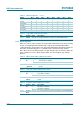
Table 20. CLKOUT control (address 0Dh) bits description
Bit Symbol Value Description
7 FE 0 the CLKOUT output is inhibited and CLKOUT output is set to
high-impedance
1 the CLKOUT output is activated
1 to 0 FD1 and
FD0
these bits control the frequency output at pin CLKOUT;
see
Table 21
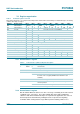
Table 21. FD1 and FD0: CLKOUT frequency selection
FD1 FD0 CLKOUT frequency
0 0 32.768 kHz
0 1 1024 Hz
1032Hz
111Hz
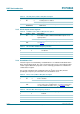
Table 22. Timer control (address 0Eh) bits description
Bit Symbol Value Description
7 TE 0 timer is disabled
1 timer is enabled
1 to 0 TD1 and
TD0
timer source clock frequency select; these bits determine the
source clock for the countdown timer, see
Table 23; when not in
use, TD1 and TD0 should be set to
1
⁄
60
Hz for power saving
Table 23. TD1 and TD0: Timer frequency selection
TD1 TD0 TIMER Source clock frequency
0 0 4096 Hz
0164Hz
101Hz
111⁄60 Hz