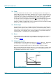
PCF8563 Real time clock/calendar Rev. 05 — 17 July 2007 Product data sheet 1. General description The PCF8563 is a CMOS real time clock/calendar optimized for low power consumption. A programmable clock output, interrupt output and voltage-low detector are also provided. All address and data are transferred serially via a two-line bidirectional I2C-bus. Maximum bus speed is 400 kbit/s. The built-in word address register is incremented automatically after each written or read data byte. 2.
PCF8563 NXP Semiconductors Real time clock/calendar 4. Ordering information Table 1. Ordering information Type number Topside mark Package Name Description Version PCF8563P PCF8563P DIP8 plastic dual in-line package; 8 leads (300 mil) SOT97-1 PCF8563T 8563T SO8 plastic small outline package; 8 leads; body width 3.
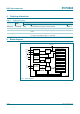
PCF8563 NXP Semiconductors Real time clock/calendar 6. Pinning information 6.1 Pinning OSCI 1 OSCO 2 8 VDD 7 CLKOUT OSCI 1 OSCO 2 8 VDD 7 CLKOUT PCF8563T PCF8563P INT 3 6 SCL INT VSS 4 5 SDA VSS 3 6 SCL 4 5 SDA 001aaf975 001aaf977 Fig 2. Pin configuration DIP8 Fig 3. Pin configuration SO8 terminal 1 index area OSCI 1 8 VDD OSCO 2 7 CLKOUT INT 3 6 SCL VSS 4 5 SDA PCF8563TS OSCI 1 10 n.c. OSCO 2 9 VDD n.c.
PCF8563 NXP Semiconductors Real time clock/calendar 6.2 Pin description Table 2. Symbol Pin description Pin Description DIP8, SO8, TSSOP8 HVSON10 OSCI 1 1 oscillator input OSCO 2 2 oscillator output n.c - 3 not connected INT 3 4 interrupt output (open-drain; active LOW) VSS 4 5 ground SDA 5 6 serial data input and output SCL 6 7 serial clock input CLKOUT 7 8 clock output, open-drain VDD 8 9 positive supply voltage n.c - 10 not connected 7.
PCF8563 NXP Semiconductors Real time clock/calendar 7.2 Timer The 8-bit countdown timer at address 0Fh is controlled by the timer control register at address 0Eh. The timer control register determines one of 4 source clock frequencies for the timer (4096 Hz, 64 Hz, 1 Hz, or 1⁄60 Hz), and enables or disables the timer. The timer counts down from a software-loaded 8-bit binary value. At the end of every countdown, the timer sets the Timer Flag (TF). The TF may only be cleared by software.
PCF8563 NXP Semiconductors Real time clock/calendar 7.6 Register organization Table 3. Formatted registers overview Bit positions labelled as x are not implemented. Bit positions labelled with 0 should always be written with logic 0; if read they could be either logic 0 or logic 1.
PCF8563 NXP Semiconductors Real time clock/calendar Bits TIE and AIE: These bits activate or deactivate the generation of an interrupt when TF or AF is asserted, respectively. The interrupt is the logical OR of these two conditions when both AIE and TIE are set. Table 5.
PCF8563 NXP Semiconductors Real time clock/calendar Table 9. Hours (address 04h) bits description Bit Symbol Value Description 5 to 0 HOURS 00 to 23 this register holds the current hours coded in BCD format Table 10. Bit 5 to 0 [1] DAYS Description [1] 01 to 31 this register holds the current day coded in BCD format The PCF8563 compensates for leap years by adding a 29th day to February if the year counter contains a value which is exactly divisible by 4, including the year 00. Table 11.
PCF8563 NXP Semiconductors Real time clock/calendar Table 14. Month assignments …continued Month Bit 7 Bit 6 Bit 5 Bit 4 Bit 3 Bit 2 Bit 1 Bit 0 July C x x 0 0 1 1 1 August C x x 0 1 0 0 0 September C x x 0 1 0 0 1 October C x x 1 0 0 0 0 November C x x 1 0 0 0 1 December C x x 1 0 0 1 0 Table 15.
PCF8563 NXP Semiconductors Real time clock/calendar Table 19. Weekday alarm (address 0Ch) bits description Bit Symbol Value Description 7 AE 0 weekday alarm is enabled 2 to 0 ALARM_ 0 to 6 WEEKDAYS 1 weekday alarm is disabled this register holds the weekday alarm information coded in BCD format 7.6.5 Clock output control register Table 20.
PCF8563 NXP Semiconductors Real time clock/calendar Table 24. Timer (address 0Fh) bits description Bit Symbol Value Description 7 to 0 TIMER 00h to FFh countdown value = n; n CountdownPeriod = --------------------------------------------------------------SourceClockFrequency 7.7 EXT_CLK test mode A test mode is available which allows for on-board testing. In such a mode it is possible to set up test conditions and control the operation of the RTC.
PCF8563 NXP Semiconductors Real time clock/calendar Once the override mode has been entered, the device immediately stops being reset and normal operation may commence i.e. entry into the EXT_CLK test mode via I2C-bus access. The override mode may be cleared by writing a logic 0 to TESTC. TESTC must be set to logic 1 before re-entry into the override mode is possible. Setting TESTC to logic 0 during normal operation has no effect except to prevent entry into the POR override mode.
PCF8563 NXP Semiconductors Real time clock/calendar 8.1 Bit transfer One data bit is transferred during each clock pulse. The data on the SDA line must remain stable during the HIGH period of the clock pulse as changes in the data line at this time will be interpreted as a control signal (see Figure 9). SDA SCL data line stable; data valid change of data allowed mbc621 Fig 9. Bit transfer 8.2 Start and stop conditions Both data and clock lines remain HIGH when the bus is not busy.
PCF8563 NXP Semiconductors Real time clock/calendar 8.4 Acknowledge The number of data bytes transferred between the START and STOP conditions from transmitter to receiver is unlimited. Each byte of eight bits is followed by an acknowledge bit. The acknowledge bit is a HIGH-level signal put on the bus by the transmitter during which time the master generates an extra acknowledge related clock pulse. A slave receiver which is addressed must generate an acknowledge after the reception of each byte.
PCF8563 NXP Semiconductors Real time clock/calendar 8.5.2 Clock/calendar read/write cycles The I2C-bus configuration for the different PCF8563 read and write cycles is shown in Figure 14, Figure 15 and Figure 16. The word address is a 4-bit value that defines which register is to be accessed next. The upper four bits of the word address are not used.
PCF8563 NXP Semiconductors Real time clock/calendar 9. Limiting values Table 26. Limiting values In accordance with the Absolute Maximum Rating System (IEC 60134) Symbol Parameter Min Max Unit VDD supply voltage −0.5 +6.5 V IDD supply current −50 +50 mA VI input voltage on pins SCL and SDA −0.5 +6.5 V input voltage on pin OSCI −0.5 VDD + 0.5 V VO output voltage on pins CLOCKOUT and INT −0.5 +6.
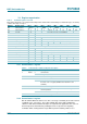
PCF8563 NXP Semiconductors Real time clock/calendar Table 27. Static characteristics …continued VDD = 1.8 V to 5.5 V; VSS = 0 V; Tamb = −40 °C to +85 °C; fosc = 32.768 kHz; quartz Rs = 40 kΩ; CL = 8 pF; unless otherwise specified. Symbol IDD3 Parameter supply current 3 Conditions Min Typ Max Unit VDD = 5.0 V - 825 1600 nA VDD = 3.0 V - 550 1000 nA - 425 800 nA VDD = 5.0 V - 950 1700 nA VDD = 3.0 V - 650 1100 nA VDD = 2.
PCF8563 NXP Semiconductors Real time clock/calendar mgr888 1 mgr889 1 IDD (mA) IDD (mA) 0.8 0.8 0.6 0.6 0.4 0.4 0.2 0.2 0 0 0 2 4 VDD (V) 6 Tamb = 25 °C; Timer = 1 minute. 0 2 4 VDD (V) 6 Tamb = 25 °C; Timer = 1 minute. Fig 17. IDD as a function of VDD; CLKOUT disabled Fig 18. IDD as a function of VDD; CLKOUT = 32 kHz mgr891 mgr890 1 IDD (mA) 4 frequency deviation (ppm) 2 0.8 0.6 0 0.4 −2 0.
PCF8563 NXP Semiconductors Real time clock/calendar 11. Dynamic characteristics Table 28. Dynamic characteristics VDD = 1.8 V to 5.5 V; VSS = 0 V; Tamb = −40 °C to +85 °C; fosc = 32.768 kHz; quartz Rs = 40 kΩ; CL = 8 pF; unless otherwise specified. Symbol Parameter Conditions Min Typ Max Unit 15 25 35 pF - 2 × 10⁻⁷ - - Oscillator CL(itg) integrated load capacitance ∆fosc/fosc relative oscillator frequency variation ∆VDD = 200 mV; Tamb = 25 °C Quartz crystal parameters (f = 32.
PCF8563 NXP Semiconductors Real time clock/calendar SDA t BUF t LOW tf SCL t HD;STA tr t HD;DAT t HIGH t SU;DAT SDA t SU;STA t SU;STO mga728 Fig 21. I2C-bus timing waveforms 12. Application information VDD SDA 1F SCL MASTER TRANSMITTER/ RECEIVER VDD SCL CLOCK CALENDAR OSCI PCF8563 OSCO VSS SDA VDD R SDA SCL (I2C-bus) R R: pull-up resistor tr R= Cb mgm665 Fig 22. Application diagram PCF8563_5 Product data sheet © NXP B.V. 2007. All rights reserved. Rev.
PCF8563 NXP Semiconductors Real time clock/calendar 12.1 Quartz frequency adjustment 12.1.1 Method 1: fixed OSCI capacitor By evaluating the average capacitance necessary for the application layout, a fixed capacitor can be used. The frequency is best measured via the 32.768 kHz signal available after power-on at pin CLKOUT. The frequency tolerance depends on the quartz crystal tolerance, the capacitor tolerance and the device-to-device tolerance (on average ±5 × 10⁻⁶).
PCF8563 NXP Semiconductors Real time clock/calendar 13. Package outline DIP8: plastic dual in-line package; 8 leads (300 mil) SOT97-1 ME seating plane D A2 A A1 L c Z w M b1 e (e 1) b MH b2 5 8 pin 1 index E 1 4 0 5 10 mm scale DIMENSIONS (inch dimensions are derived from the original mm dimensions) UNIT A max. A1 min. A2 max. b b1 b2 c D (1) E (1) e e1 L ME MH w Z (1) max. mm 4.2 0.51 3.2 1.73 1.14 0.53 0.38 1.07 0.89 0.36 0.23 9.8 9.2 6.48 6.20 2.54 7.
PCF8563 NXP Semiconductors Real time clock/calendar SO8: plastic small outline package; 8 leads; body width 3.9 mm SOT96-1 D E A X c y HE v M A Z 5 8 Q A2 A (A 3) A1 pin 1 index θ Lp 1 L 4 e detail X w M bp 0 2.5 5 mm scale DIMENSIONS (inch dimensions are derived from the original mm dimensions) UNIT A max. A1 A2 A3 bp c D (1) E (2) e HE L Lp Q v w y Z (1) mm 1.75 0.25 0.10 1.45 1.25 0.25 0.49 0.36 0.25 0.19 5.0 4.8 4.0 3.8 1.27 6.2 5.8 1.05 1.0 0.
PCF8563 NXP Semiconductors Real time clock/calendar TSSOP8: plastic thin shrink small outline package; 8 leads; body width 3 mm D E SOT505-1 A X c y HE v M A Z 5 8 A2 pin 1 index (A3) A1 A θ Lp L 1 4 detail X e w M bp 0 2.5 5 mm scale DIMENSIONS (mm are the original dimensions) UNIT A max. A1 A2 A3 bp c D(1) E(2) e HE L Lp v w y Z(1) θ mm 1.1 0.15 0.05 0.95 0.80 0.25 0.45 0.25 0.28 0.15 3.1 2.9 3.1 2.9 0.65 5.1 4.7 0.94 0.7 0.4 0.1 0.1 0.1 0.70 0.
PCF8563 NXP Semiconductors Real time clock/calendar HVSON10: plastic thermal enhanced very thin small outline package; no leads; 10 terminals; body 3 x 3 x 0.85 mm SOT650-1 0 1 2 mm scale X A B D A A1 E c detail X terminal 1 index area C e1 terminal 1 index area e 5 y y1 C v M C A B w M C b 1 L Eh 6 10 Dh DIMENSIONS (mm are the original dimensions) UNIT A(1) max. A1 b c D(1) Dh E(1) Eh e e1 L v w y y1 mm 1 0.05 0.00 0.30 0.18 0.2 3.1 2.9 2.55 2.15 3.1 2.
PCF8563 NXP Semiconductors Real time clock/calendar 14. Handling information Inputs and outputs are protected against electrostatic discharge in normal handling. However, to be completely safe you must take normal precautions appropriate to handling MOS devices; see JESD625-A and/or IEC61340-5. 15. Soldering This text provides a very brief insight into a complex technology. A more in-depth account of soldering ICs can be found in Application Note AN10365 “Surface mount reflow soldering description”.
PCF8563 NXP Semiconductors Real time clock/calendar • Process issues, such as application of adhesive and flux, clinching of leads, board transport, the solder wave parameters, and the time during which components are exposed to the wave • Solder bath specifications, including temperature and impurities 15.
PCF8563 NXP Semiconductors Real time clock/calendar temperature maximum peak temperature = MSL limit, damage level minimum peak temperature = minimum soldering temperature peak temperature time 001aac844 MSL: Moisture Sensitivity Level Fig 27. Temperature profiles for large and small components For further information on temperature profiles, refer to Application Note AN10365 “Surface mount reflow soldering description”. PCF8563_5 Product data sheet © NXP B.V. 2007. All rights reserved. Rev.
PCF8563 NXP Semiconductors Real time clock/calendar 16. Revision history Table 31. Revision history Document ID Release date Data sheet status Change notice Supersedes PCF8563_5 20070717 Product data sheet - PCF8563-04 Modifications: PCF8563-04 (9397 750 12999) Modifications: • The format of this data sheet has been redesigned to comply with the new identity guidelines of NXP Semiconductors. • • • • • Legal texts have been adapted to the new company name where appropriate.
PCF8563 NXP Semiconductors Real time clock/calendar 17. Legal information 17.1 Data sheet status Document status[1][2] Product status[3] Definition Objective [short] data sheet Development This document contains data from the objective specification for product development. Preliminary [short] data sheet Qualification This document contains data from the preliminary specification. Product [short] data sheet Production This document contains the product specification.
PCF8563 NXP Semiconductors Real time clock/calendar Notes PCF8563_5 Product data sheet © NXP B.V. 2007. All rights reserved. Rev.
PCF8563 NXP Semiconductors Real time clock/calendar 19. Contents 1 2 3 4 5 6 6.1 6.2 7 7.1 7.2 7.3 7.4 7.5 7.6 7.6.1 7.6.2 7.6.3 7.6.4 7.6.5 7.6.6 7.7 7.8 8 8.1 8.2 8.3 8.4 8.5 8.5.1 8.5.2 9 10 11 12 12.1 12.1.1 12.1.2 12.1.3 13 14 15 15.1 15.2 15.3 General description . . . . . . . . . . . . . . . . . . . . . . 1 Features . . . . . . . . . . . . . . . . . . . . . . . . . . . . . . . 1 Applications . . . . . . . . . . . . . . . . . . . . . . . . . . . . 1 Ordering information . . . . . . . . . . . . . .