F815D Series (Full-Size Single Board Computer) INSTALLATION GUIDE Installation Guide Revision A2 6007002815DA2
COPYRIGHT© All rights reserved. The information contained in this guide has been validated and reviewed for accuracy. No patent liability is assumed with respect to the use of the information contained herein. While every precaution has been taken in the preparation of this guide, the Manufacturer assumes no responsibility for errors or omissions.
CONTENTS SECTION 1 INTRODUCTION 1.1 Unpacking F815D Series 1.2 Description 1.3 Features 1.3.1 Hardware Monitoring 1.3.2 I/O Shield Connector 1.3.3 F815D Series Overview 1.3.4 System Block Diagram 1.4 Specifications 1 1 3 3 4 4 4 5 6 SECTION 2 INSTALLATIONS 2.1 System Installation 2.1.1 CPU Installation 2.1.2 Memory Module Installation 2.1.3 Setting Jumpers 2.2 Board Layout 2.3 Jumper Setting 2.
CONTENTS SECTION 3 AWARD BIOS SETUP 3.1 BIOS Instructions 3.2 Main Menu 3.3 Standard CMOS Features 3.4 IDE Adapters 3.5 Advanced BIOS Features 3.6 Advanced Chipset Features 3.7 Integrated Peripherals 3.8 Power Management Setup 3.9 PnP/PCI Configurations 3.10 PC Health Status 3.11 Frequency/Voltage Control 3.12 Load Fail-Safe Default 3.13 Load Optimized Defaults 3.14 Supervisor/User Password Setting 3.
iv
SECTION 1 INTRODUCTION 1.1 Unpacking F815D Series 1. Take out the F815D series unit from the carton box, check if the unit is properly secure in the plastic bag. 2.
Introduction ¡ ATX power control cable (4-pins to 4-pins) ¡ K/B-M/S extend to BP cable (6-pins to 6-pins) ¡ Driver CD 3. Optional Cable ¡ USB1.
Introduction 1.2 Description The F815D Series single board computer is optimized for socket 370 FC-PGA processor, supporting 100MHz and 133 MHz Front Side Bus, the memory can accommodate is up to 512 MB SDRAM. This board is based on the Intel® 815EP/E chipset and is fully designed for harsh industrial environment. The F815D/V series is with on-die VGA function. The F815D series is one pure SBC. Them are for entry-level applications.
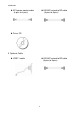
Introduction 1.3.1 Hardware Monitoring Hardware monitoring allows you to monitor various aspects of your systems operations and status. The features include CPU temperature, voltage and RPM of fan. 1.3.2 I/O Shield Connector The SBC is equipped with an I/O bracket. Please use the appropriate I/O shield (figure 1). F815D Series F815D/V Series Figure 1: I/O bracket layout 1.3.
Introduction 1.3.
Introduction 1.
Introduction ¡ Extended Function: - Hardware Monitoring function by W83781D - IrDA by pin-header ¡ Form Factor: - 13.3” x 4.8” (338 x 122mm) ¡ Weight: - 0.84lb (380 g.w.) --- F815D/V - 0.88lb (400 g.w.
SECTION 2 INSTALLATIONS 2.1 System Installation 2.1.1 CPU Installation Carefully follow the steps below in order to install the CPU: 1. Check and confirm that you are going to install correctly CPU type and pin numbers (figure 3). 2. Lift the releasing lever of the Socket 370. 3. Align the pin of the CPU against the pinholes of the Socket 370. Be sure to pay attention to the orientation of the CPU. Figure 3: CPU Socket 4. Push down the CPU into the Socket 370. 5.
Installations Removing a CPU: 1. Before removing the CPU, turn off the F815D Series power; then wait for about 20 minutes until the heat radiation plate of the cooling fan and the CPU cool down. 2. To remove the CPU, lift the releasing lever of the Socket 370. Note: The CPU and the heat radiation plate are hot. They may cause burns. To remove the CPU, reverse the installation steps. 2.1.2 Memory Module Installation Figure 4 display the notch marks and what they should look like on your DIMM memory module.
Installations Carefully follow the steps below in order to install the DIMMs: 1. To avoid generating static electricity and damaging the DIMM, ground yourself by touching a grounded metal surface or using a ground scrap before you touch the DIMM. 2. Do not touch the connector of the DIMM. Dirt residue may cause a malfunction. 3. Hold the DIMM with its notch to the front side of the F815D Series and insert it completely into the socket. A DIMM should be inserted into the inner socket first.
Installations 2.1.3 Setting Jumpers There are jumpers on the system board of the F815D Series. You can set the jumpers to make the necessary operations. Figure 6: Jumper Connector For any three-pins jumpers (Figure 6), the jumper setting is 1-2 when the jumper connects pin 1 and 2. The setting is 2-3 when pin 2 and 3 are connected and so on. You see one of the lines surrounding jumpers is thick, which indicates pin NO.1.
Installations Board Layout Jumper & Connector Location CN4 CN21 CN22 CN14 CN19 CN17 JP1 CN9 CN10 CN12 CN15 CN3 CN7 JP2 IDE2 IDE1 JP3 CN2 CN6 BAT1 DIMM2 DIMM1 2.2 CN18 CN20 BZ1 CN1 CN5 CN8 CN11 F815D REV1.
Installations 2.3 Jumper Setting Table for Jumper Location Description: Use the information in the following table to change the jumpers.
Installations In order to set up the correct configuration, here is the description about how to set the jumpers to enable/disable or change functions. All jumpers’ location please refer to jumper location diagram. COM port setting select: JP1 JP1 Function RS-232 (Default) RS-422 RS-485 1-2 Off On (Term.) On On (Term.) On 3-4 Off (Term.) (Term.
Installations Watchdog Timer setting select: JP3 Function NMI Reset System (Default) JP3 1-2 2-3 y Location: 15
Installations Connector’s Description Connector Location CN4 CN21 CN22 CN14 CN19 CN17 JP1 CN9 CN10 CN12 CN15 CN3 CN7 JP2 IDE2 IDE1 JP3 CN2 CN6 BAT1 DIMM2 DIMM1 2.4 CN18 CN20 BZ1 CN1 CN5 CN8 CN11 F815D REV1.
Installations Table for Connector’s Location Description: Use the information in the following table to change the connector.
Installations Secondary IDE connector (40-pins 2.
Installations Parallel port connector (26-pins 2.
Installations Primary IDE connector (40-pins 2.
Installations Floppy disk connector (34-pins 2.
Installations COM2 RS-232 serial port connector (10-pins 2.54mm pitch pin-Header with housing): CN9 Pin # Assignment Pin # Assignment 1 3 5 7 9 DCD (Data Carrier Detect) RXD (Receive Data) TXD (Transmit Data) DTR (Data Terminal Ready) Ground 2 4 6 8 10 DSR (Data Set Ready) RTS (Request to Send) CTS (Clear to Send) RI (Ring Indicator) NC y Figure: 9 1 10 2 COM2 RS-422/485 serial port connector (10-pins 2.
Installations System panel indicate connector: CN11 Pin # Assignment Pin # IR 1 3 5 7 9 +5V FIRTX IRRX Ground IRTX 2 4 SPEAKER HDLED+ HDLED- SPKR (Default) BUZZ (Default) Ground +5V PWR LED PWR ON 23 25 RESET+ Ground 8 10 12 14 HDD LED 13 15 Assignment RESET 18 20 22 VCC PWRBT- PWLED+ NC Ground KEYLOCK 24 26 KBLOCK Ground y Figure: 25 1 26 2 USB3/USB4 port connectors (10-pins pin-header): CN12 Pin # Assignment Pin # Assignment 1 3 5 7 9 VCC USB3 USB3 + Ground Ground 2 4 6 8 10 G
Installations PS/2 mouse connector (Mini Din 6-pins): CN14 Pin # Assignment Pin # 1 3 5 Mouse Data Ground Mouse Clock Assignment 2 4 6 NC +5V NC y Figure: 6 5 4 3 2 1 USB1/USB2 port connectors (10-pins pin-header): CN15 Pin # Assignment Pin # Assignment 1 3 5 7 9 VCC USB1 USB1 + Ground Ground 2 4 6 8 10 Ground Ground USB2 + USB2 VCC y Figure: 24 9 1 10 2
Installations External keyboard & mouse connector (6-pins): CN17 Pin # Assignment 1 2 3 4 5 6 Mouse Clock Mouse Data Keyboard Clock Keyboard Data Ground +5V y Figure: 6 1 System fan power connector: CN18 Pin # 1 2 3 Assignment Ground +12V Fan Status Signal y Figure: 1 25 3
Installations PS/2 keyboard connector (Mini Din 6-pins): CN19 Pin # Assignment Pin # Assignment 1 3 5 Keyboard Data Ground Keyboard Clock 2 4 6 NC +5V NC y Figure: 6 5 4 3 2 CPU fan connector: CN20 Pin # 1 Assignment 1 2 3 Ground +12V Fan Status Signal y Figure: 1 26 3
Installations COM1 RS-232 serial port connector (D-SUB 9-pins male): CN21 Pin # Assignment Pin # Assignment 1 2 3 4 5 DCD (Data Carrier Detect) RXD (Receive Data) TXD (Transmit Data) DTR (Data Terminal Ready) Ground 6 7 8 9 DSR (Data Set Ready) RTS (Request to Send) CTS (Clear to Send) RI (Ring Indicator) y Figure: 5 1 9 6 CRT VGA (F815D/V Series only) port connector (D-SUB 15-pins female): CN22 Pin # Assignment Pin # Assignment 1 3 5 7 9 11 13 15 Red Color Signal Blue Color Signal Ground Grou
Installations COM2 (F815D Series only) serial port connector (D-SUB 9-pins male): CN22 Pin # Assignment Pin # Assignment 1 3 5 7 9 DCD (Data Carrier Detect) TXD (Transmit Data) Ground RTS (Request to Send) RI (Ring Indicator) 2 4 6 8 10 RXD (Receive Data) DTR (Data Terminal Ready) DSR (Data Set Ready) CTS (Clear to Send) NC y Figure: 5 1 9 6 Note: If user want to uses the RS-232 on COM2 port, that user must connect the cable to the location CN9 connector.
SECTION 3 AWARD BIOS SETUP 3.1 BIOS Instructions Award’s ROM BIOS provides a built-in Setup program, which allows user to modify the basic system configuration and hardware parameters. The modified data will be stored in a battery-backed CMOS, so that data will be retained even when the power is turned off. In general, the information saved in the CMOS RAM will stay unchanged unless there is a configuration change in the system, such as hard drive replacement or a device is added.
Award BIOS Setup 3.2 Main Menu Once you enter the AwardBIOS™ CMOS Setup Utility, the Main Menu will appear on the screen. The Main Menu allows you to select from several setup functions and two exit choices. Use the arrow keys to select among the items and press to accept and enter the sub-menu.
Award BIOS Setup Integrated Peripherals: Use this menu to specify your settings for integrated peripherals. See section 3.7 for the details. Power Management Setup: Use this menu to specify your settings for power management. See 3.8 for the details. PnP / PCI Configuration: This entry appears if your system supports PnP / PCI. See 3.9 for the details. PC Health Status: Use this menu to show your system temperature, speed and voltage status. See 3.10 for the details.
Award BIOS Setup 3.3 Standard CMOS Features The items in Standard CMOS Setup Menu are divided into 10 categories. Each category includes no, one or more than one setup items. Use the arrow keys to highlight the item and then use the or keys to select the value you want in each item.
Award BIOS Setup IDE Secondary Master: Options are in its sub menu (described in Table 3) Press to enter the sub menu of detailed options. IDE Secondary Slave: Options are in its sub menu (described in Table 3) Press to enter the sub menu of detailed options. Drive A/ Drive B: Options None 360K, 5.25 in/1.2M, 5.25 in/720K, 3.5 in/ 1.44M, 3.5 in/2.88M, 3.5 in Select the type of floppy disk drive installed in your system.
Award BIOS Setup 3.4 IDE Adapters The IDE adapters control the hard disk drive. Use a separate sub menu to configure each hard disk drive. CMOS Setup Utility – Copyright © 1984 - 2001 Award Software IDE Primary Master IDE HDD Auto-Detection Press Enter Item Help ____________________________ IDE Primary Master Access Mode Auto 2557 MB Auto Menu Level Cylinder Head Precomp Landing Zone Sector 4956 16 0 4955 63 ¾¾ To auto-detect the HDD’s size, head...
Award BIOS Setup The following options are selectable only if the ‘IDE Primary Master’ item is set to ‘Manual’ Cylinder: Options Min = 0, Max = 65535 Set the number of cylinders for this hard disk.
Award BIOS Setup 3.5 Advanced BIOS Features This section allows you to configure your system for basic operation. You have the opportunity to select the system’s default speed, boot-up sequence, keyboard operation, shadowing and security.
Award BIOS Setup Enabled---Activates automatically when the system boots up causing a warning message to appear when anything attempts to access the boot sector or hard disk partition table. Disabled---No warning message will appear when anything attempts to access the boot sector or hard disk partition table. CPU Internal Cache/External Cache: These two categories speed up memory access. However, it depends on CPU/chipset design.
Award BIOS Setup Boot Up Floppy Seek: Seeks disk drives during boot up. Disabling speeds boot up. The choice: Enabled, Disabled. Boot Up NumLock Status: Select power on state for NumLock. The choice: On, Off Gate A20 Option: Select if chipset or keyboard controller should control GateA20. Normal---A pin in the keyboard controller controls GateA20 Fast---Lets chipset control GateA20 Typematic Rate Setting: Keystrokes repeat at a rate determined by the keyboard controller.
Award BIOS Setup Note: To disable security, select PASSWORD SETTING at Main Menu and then you will be asked to enter password. Do not type anything and just press , it will disable security. Once the security is disabled, the system will boot and you can enter Setup freely. OS Select For DRAM > 64MB: Select the operating system that is running with greater than 64MB of RAM on the system. The choice: Non-OS2, OS2. HDD S.M.A.R.T. Capability: Enabled SMART hard driver functions for compatible.
Award BIOS Setup 3.6 Advanced Chipset Features This section allows you to configure the system based on the specific features of the installed chipset. This chipset manages bus speeds and access to system memory resources, such as DRAM and the external cache. It also coordinates communications between the conventional ISA bus and the PCI bus. It must be stated that these items should never need to be altered.
Award BIOS Setup SDRAM RAS-to-CAS Delay: You can select RAS to CAS Delay time in HCLKs of 2/2 or 3/3. The system board designer should set the values in this field, depending on the DRAM installed. Do not change the values in this field unless you change specifications of the installed DRAM or the installed CPU. The choice: 2, 3 and Auto.
Award BIOS Setup Delayed Transaction: The chipset has an embedded 32-bit posted write buffer to support delay transactions cycles. Select “Enabled” to support compliance with PCI specification version 2.1. The choice: Enabled, Disabled. AGP Graphics Aperture Size: This field determines the effective size of the Graphic Aperture used for a particular GMCH configuration. It can be updated by the GMCH-specific BIOS configuration sequence before the PCI standard bus enumeration sequence takes place.
Award BIOS Setup 3.
Award BIOS Setup IDE Primary/Secondary Master/Slave PIO: The four IDE PIO (Programmed Input/Output) fields let you set a PIO mode (0-4) for each of the four IDE devices that the onboard IDE interface supports. Modes 0 through 4 provide successively increased performance. In Auto mode, the system automatically determines the best mode for each device. The choice: Auto, Mode 0, Mode 1, Mode 2, Mode 3 and Mode 4.
Award BIOS Setup IDE HDD Block Mode: Block mode is also called block transfer, multiple commands, or multiple sector read/write. If your IDE hard drive supports block mode (most new drives do), select Enabled for automatic detection of the optimal number of block read/writes per sector the drive can support. The choice: Enabled, Disabled KBC Input Clock: This item allows you to adjust the keyboard input clock. The choice: 8MHz, 12MHz.
Award BIOS Setup Use IR Pins: This item allows you to select IR transmission routes, one is RxD2m, TxD2 (COM Port) and the other is IR-Rx2Tx2. The choice: IR-Rx2Tx2, RxD2 and TxD2. Onboard Parallel Port: This item allows you to determine access onboard parallel port controller with which I/O address. The choice: 3BC/IRQ7, 378/IRQ7, 278/IRQ5 and Disabled. Parallel Port Mode: Select an operating mode for the onboard parallel (printer) port.
Award BIOS Setup 3.8 Power Management Setup The Power Management Setup allows you to configure you system to most effectively save energy while operating in a manner consistent with your own style of computer use.
Award BIOS Setup 1. HDD Power Down 2. Doze Mode 3. Suspend Mode Min. Power Saving: Minimum power management. Doze Mode = 1 hr. Standby Mode = 1 hr., Suspend Mode = 1 hr., and HDD Power Down = 15 min. Max. Power Saving: Maximum power management -- ONLY AVAILABLE FOR SL CPU’s. Doze Mode = 1 min., Standby Mode = 1 min., Suspend Mode = 1 min., and HDD Power Down = 1 min. User Defined: Allow you to set each mode individually. When not disabled, each of the ranges is from 1 min. to 1 hr.
Award BIOS Setup MODEM Use IRQ: This determines the IRQ in which the MODEM can use. The choice: 3, 4, 5, 7, 9, 10, 11 and NA. Suspend Mode: When “Enabled” and after the set time of system inactivity. All devices except the CPU will be shut off. The choice: Enabled, Disabled. HDD Power Down: When “Enabled” and after the set time of system inactivity, the hard disk drive will be powered down while all other devices remain active. The choice: Enabled, Disabled.
Award BIOS Setup PM Events: PM events are I/O events whose occurrence can prevent the system from entering a power saving mode or can awaken the system from such a mode. In effect, the system remains alert for anything, which occurs to a device, which is configured as Enabled, even when the system is in a power down mode.
Award BIOS Setup 3.9 PnP/PCI Configurations This section describes configuring the PCI bus system. PCI, or Personal Computer Interconnect, is a system, which allows I/O devices to operate at speeds nearing the speed the CPU itself uses when communicating with its own special components. This section covers some very technical items and it is strongly recommended that only experienced users should make any changes to the default settings.
Award BIOS Setup Resource controlled by: The Award Plug and Play BIOS has the capacity to automatically configure all of the boot and Plug and Play compatible devices. However, this capability means absolutely nothing unless you are using a Plug and Play operating system such as Windows®95. If you set this field to “Manual” choose specific resources by going into each of the sub menu that follows this field (a sub menu is preceded by a “¾”). The choice: Auto (ESCD), Manual.
Award BIOS Setup 3.10 PC Health Status CMOS Setup Utility – Copyright © 1984 - 2001 Award Software PC Health Status CPU Warning Temperature Current System Temp. Current CPU Temp. Current Chassis Fan Speed Current CPU Fan Speed Vtt (V) Vcore (V) +3.3V +5V +12 V -12 V -5V VBAT (V) 5VSB (V) Shutdown temperature Disabled 57°C/134°F 28°C/82°F 5273RPM 4687RPM 1.47V 1.64V 3.28V 4.94V 12.09V -11.37V -5.09V 3.04V 4.
Award BIOS Setup +3.3V/+5V/+12V/-12V/-5V: Show you the voltage of +3.3V/+5V/+12V/-12V/-5V. Shutdown Temperature: This item allows you to set up the CPU shutdown Temperature. The choice: Disabled, 60°C / 140°F, 65°C / 149°F, 70°C / 159°F and 75°C / 167°F.
Award BIOS Setup 3.
Award BIOS Setup CPU Clock Ratio: This item allows you to set up the CPU clock ratio, but this function depends on different CPU performance. It is only effective for those clock ratio haven’t been locked. The choice: X3.0 ~ X8.0.
Award BIOS Setup 3.12 Load Fail-Safe Defaults When you press on this item you get a confirmation dialog box with a message similar to: Load Fail-Safe Defaults (Y/N)? N Pressing “Y” loads the BIOS default values for the most stable, minimal-performance system operations.
Award BIOS Setup 3.13 Load Optimized Defaults When you press on this item you get a confirmation dialog box with a message similar to: Load Optimized Defaults (Y/N)? N Pressing “Y” loads the default values that are factory settings for optimal performance system operations.
Award BIOS Setup 3.14 Supervisor/User Password Setting You can set either supervisor or user password, or both of then. The differences between are: Set Supervisor Password: can enter and change the options of the setup menus. Set User Password: just can only enter but do not have the right to change the options of the setup menus. When you select this function, the following message will appear at the center of the screen to assist you in creating a password.
Award BIOS Setup 3.15 Exit Selecting Save & Exit Setup Pressing on this item asks for confirmation: Save to CMOS and EXIT (Y/N)? Y Pressing “Y” stores the selections made in the menus in CMOS – a special section of memory that stays on after you turn your system off. The next time you boot your computer, the BIOS configures your system according to the Setup selections stored in CMOS. After saving the values the system is restarted again.