
User's Manual

SDC-WB40NBT User’s Guide
14
SDC-WB40NBT_UsersGuide
© 2011 – 2012 Summit Data Communications, Inc. All rights reserved.
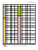
Section
Pin
No.
Pin Name
I/O
Reference
Description
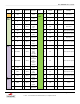
Section
Pin
No.
Pin Name
I/O
Reference
Description
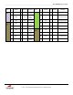
15
SPI1_CLK
O
VCC3_3
SPI
Programmin
g
Clock
16
PC25/
BOOT2
I
VCC3_3
Bootloader console
redirection to UART1;
Active low
Ethernet
RMII
17
GND
Signal
Ground
LED
18
LED0
O
VCC3_3
WLAN activity indicator
IOH = 2mA max (VDDIO
= 1.8V)
IOH = 4mA max (VDDIO
= 3.3V)
19
EREFCK
I
VCC3_3
Ethernet
Reference
Clock (50
MHz max)
20
LED1
O
VCC3_3
General purpose LED1
out; Active low
21
GND
VCC3_3
Signal
Ground
22
LED2
O
VCC3_3
General purpose LED2
out; Active low
23
ETX0
O
VCC3_3
Ethernet
data
output 0
Status
24
STAT0
O
VCC3_3
Status
High while system in
reset, bootloader or OS
boot, low when OS is up
25
ETX1
O
VCC3_3
Ethernet
data
output 1
26
STAT1
O
VCC3_3
Status
High while system
running, low while
system in suspend state
27
GND
Signal
Ground
Control
28
/PWDN
I
VCC3_3
Powers down the
module, active low; 4.7K
pull-up resistor to VDDIO
is recommended
29
ERX0
I
VCC3_3
Ethernet
data
input 1
30
/RESET
I/O
VCC3_3
When the AT91 CPU is
powered on, there's a
routine in the bootloader
that asserts a reset on
the SYS_RST_L line for
100us. This resets
peripheral circuitry that
may also be attached to
the SYS_RST_L line.
31
ERX1
I
VCC3_3
Ethernet
data
input 1
Two Wire
Interface
32
GND
Signal Ground
33
GND
Signal
Ground
34
TWD
I/O
VCC3_3
Two-wire Serial Data
35
ETXEN
O
VCC3_3
Ethernet
Transmit
Enable
36
TWCK
I/O
VCC3_3
Two-wire Serial Clock
37
ECRSDV
I
VCC3_3
Ethernet
Carrier
Sense
and Data
Valid
UART1
(DCE)
38
GND
Signal Ground