
User's Manual

SDC-WB40NBT User’s Guide
13
SDC-WB40NBT_UsersGuide
© 2011 – 2012 Summit Data Communications, Inc. All rights reserved.
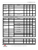
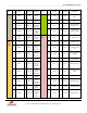
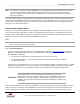
Pin Definitions
Note: Unused pins should be left open. All GND pin shall be connected to system ground.
Note: The maximum output current is 8 mA except for the following pins (which have a maximum output current
of 2 mA): 3, 4, 6, 8, 14, 16, 41, 47, 72, 87, and 89.
Note: The SDC-WB40NBT schematic is available from the Summit website.
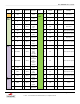
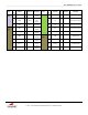
Section
Pin
No.
Pin Name
I/O
Reference
Description
Section
Pin
No.
Pin Name
I/O
Reference
Description
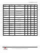
SPI
1
GND
Signal
Ground
GPIO
2
GPIO_1/
ADC0
I/O
VCC3_3
General Purpose I/O
3
SPI1_NPCS_1
O
VCC3_3
SPI 1
Peripheral
Chip Select
1
4
GPIO_2/
ADC1
I/O
VCC3_3
General Purpose I/O
5
SPI1_NPCS_0
O
VCC3_3
SPI 1
Peripheral
Chip Select
0
6
PC22
I
VCC3_3
Reserved for input to BT
device. Indicates that
Bluetooth is transmitting
or receiving high priority
packets (i.e., SCO and
LMP). Not currently
supported in the
firmware. Tie to GND
when not in use.
7
GND
Signal
Ground
8
PC23
O
VCC3_3
Output to BT device.
Indicates that the WLAN
is transmitting or
receiving high priority
packets. Not currently
supported in the
firmware. Tie to GND
when not in use.
9
SPI1_MOSI
O
VCC3_3
SPI 1 Master
Out/Slave In
UART2
(Console)
10
DRXD
I
VCC3_3
Console/Debug Serial
Input
12
DTXD
O
VCC3_3
Console/Debug Serial
Output
11
SPI1_MISO
I
VCC3_3
SPI 1 Master
In/Slave Out
Boot
Control
13
GND
Signal
Ground
14
PC24/
BOOT1
I
VCC3_3
Emergency update
initiation; Active low