
User's Manual
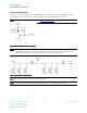
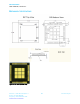
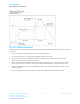
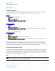
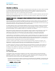
Table Of Contents

SDC-SSD40NBT
User’s Manual, version 4.1
Americas: +1-800-492-2320 Option 3
Europe: +44-1628-858-940
Hong Kong: +852-2268-6567 x026
www.lairdtech.com/wireless
26
Laird Technologies
Note: The following information results from Summit’s experience in producing the SDC-MSD40NBT.
Summit provides these data for informational purposes only and provides no warranties or claims
with regard to the applicability of this information to a particular design.
Solder Stencil Opening for Pads (56 signal pads): 1:1 to 1:0.9 (dependent on solder type)
Solder Stencil Opening for Thermal Pads (9 “window pane” pads): 1:0.5 to 1:0.75 (dependent on solder type)
Note: The vias that are in the thermal pad (6x6 pattern of 12 mil holes)
are open; they are not tented by the solder mask on the bottom
side. This allows excess paste to escape from the bottom side to
help ensure a flat SIP installation.
Solder Paste Type: No-Clean as the soldered part to board clearance will
not allow for adequate post solder cleaning.
Rework is technically challenging due to parts on the SIP reflowing at the same temperature needed for
rework. The SDC-SSD40NBT cannot be lifted by the shield during rework. As such, removal of part for rework
is not recommended. Reflow without removal has been successfully used to clear shorts found during x-ray
inspection.
Reflow: The SDC-SSD40NBT is RoHS compliant and as such is sensitive to heat. The below graphic details a
typical profile for such and device and is provided for reference purposes.
Recommendations:
If the SSD40NBT has been removed from the moisture-protective packaging for more than 24 hours, bake at
125 degrees Celsius for 24 hours (per Jedec-STD-033). This is a preparatory step prior to reflow to ensure that
the SIPs are sufficiently dehydrated. Reflow should occur immediately following baking to prevent
rehydration.
Figure 11: Footprint from the
Summit MSD30/40 PCB