
User's Manual
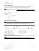
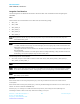
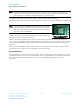
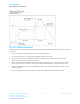
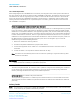
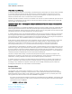
Table Of Contents

SDC-SSD40NBT
User’s Manual, version 4.1
Americas: +1-800-492-2320 Option 3
Europe: +44-1628-858-940
Hong Kong: +852-2268-6567 x026
www.lairdtech.com/wireless
22
Laird Technologies
Electrical Considerations
Below is a section of the schematic for the MSD40NBT, a PCB module based on the SSD40NBT. Summit
provides this for your reference only to aid you in integrating the SSD40NBT into your device.
Note: The full MSD40NBT schematic is located in
Appendix A: Schematic
.
Figure 8: Recommended circuit for SYS_RST_L
Note: In the reset circuit, the diode is placed in parallel with the resistor to ensure the capacitor is
discharged quickly when a power drop occurs. This minimizes the chance of register corruption
within the processor and Wi-Fi module should such a power supply glitch arise.
Figure 9: Recommended supply bypass
Note: The 10uF bypass capacitors must be a low-ESR type.
Note: The 0 ohm resistors are optional and could be replaced by a chip ferrite bead, if desired.
VCC 3.3V
VCC 3.3V