
User's Manual
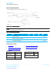
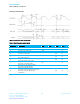
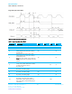
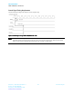
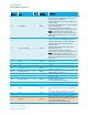
Table Of Contents

SDC-SSD40NBT
User’s Manual, version 4.1
Americas: +1-800-492-2320 Option 3
Europe: +44-1628-858-940
Hong Kong: +852-2268-6567 x026
www.lairdtech.com/wireless
11
Laird Technologies
SDIO Timing Requirements
The following figure (Figure 2) and table display SDIO default mode timing.
Figure 1: SDIO Default Mode Timing
Note: Timing is based on CL ≤ 40pF load on CMD and Data.
Table 3: SDIO Timing Requirements
Symbol
Parameter
Min
Typ
Max
Unit
SDIO CLK (All values are referred to minimum VIH and maximum VIL*)
fPP
Frequency – Data Transfer mode
0
-
25
MHz
fOD
Frequency – Identification mode
0
-
400
kHz
tWL
Clock low time
10
-
-
ns
tWH
Clock high time
10
-
-
ns
tTLH
Clock rise time
-
-
10
ns
tTHL
Clock low time
-
-
10
ns
Inputs: CMD, DAT (referenced to CLK)
tISU
Input setup time
5
-
-
ns
tIH
Input hold time
5
-
-
ns
Outputs: CMD, DAT (referenced to CLK)
tODLY
Output delay time – Data Transfer mode
0
-
14
ns
tODLY
Output delay time – Identification mode
0
-
50
ns
* min(Vih) = 0.7 x VDDIO and max(ViL) = 0.2 x VDDIO.