
User's Manual

Summit User’s Guide – SDC-SSD40L
8
SDC-SSD40L_UsersGuide
© 2011 – 2012 Summit Data Communications, Inc. All rights reserved.
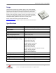
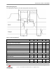
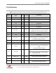
SDIO Timing Diagrams
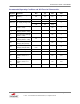
The following figure (Figure 2) and table display SDIO default mode timing.
Figure 1: SDIO Timing Diagram
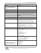
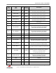
Parameter
Symbol
Min
Typical
Max
Unit
Clock CLK (All values are referred to min. VIH and max. VIL)
Frequency – Data Transfer Mode
fPP
0
-
25
MHz
Frequency – Identification Mode
fOD
0
-
400
kHz
Clock Low Time
tWL
10
-
-
ns
Clock High Time
tWH
10
-
-
ns
Clock Rise Time
tTLH
-
-
10
ns
Clock Low Time
tTHL
-
-
10
ns
Inputs: CMD, DAT (referenced to CLK)
Input Setup Time
tISU
5
-
-
ns
Input Hold Time
tIH
5
-
-
ns
Outputs: CMD, DAT (referenced to CLK)
Output Delay time – Data Transfer Mode
tODLY
0
-
14
ns
Output Delay time – Identification Mode
tODLY
0
-
50
ns