
User's Manual

Summit User’s Guide – SDC-SSD40L
17
SDC-SSD40L_UsersGuide
© 2011 – 2012 Summit Data Communications, Inc. All rights reserved.
B. PCB layout considerations
The PCB board stack is shown below using 2-Layer FR4, lead-free solder finish plating, green solder
mask on both sides and white silkscreen on both sides.
Gerber files are shown below in detail.
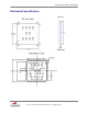
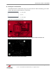
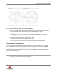
Figure 2: Components placement and trace route on the top layer. Via hole is of 10 mils size
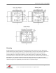
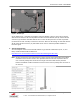
Figure 3: Components location of the top layer