
Data Sheet
%
2. Pin Definitions
2. Pin Definitions
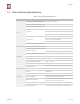
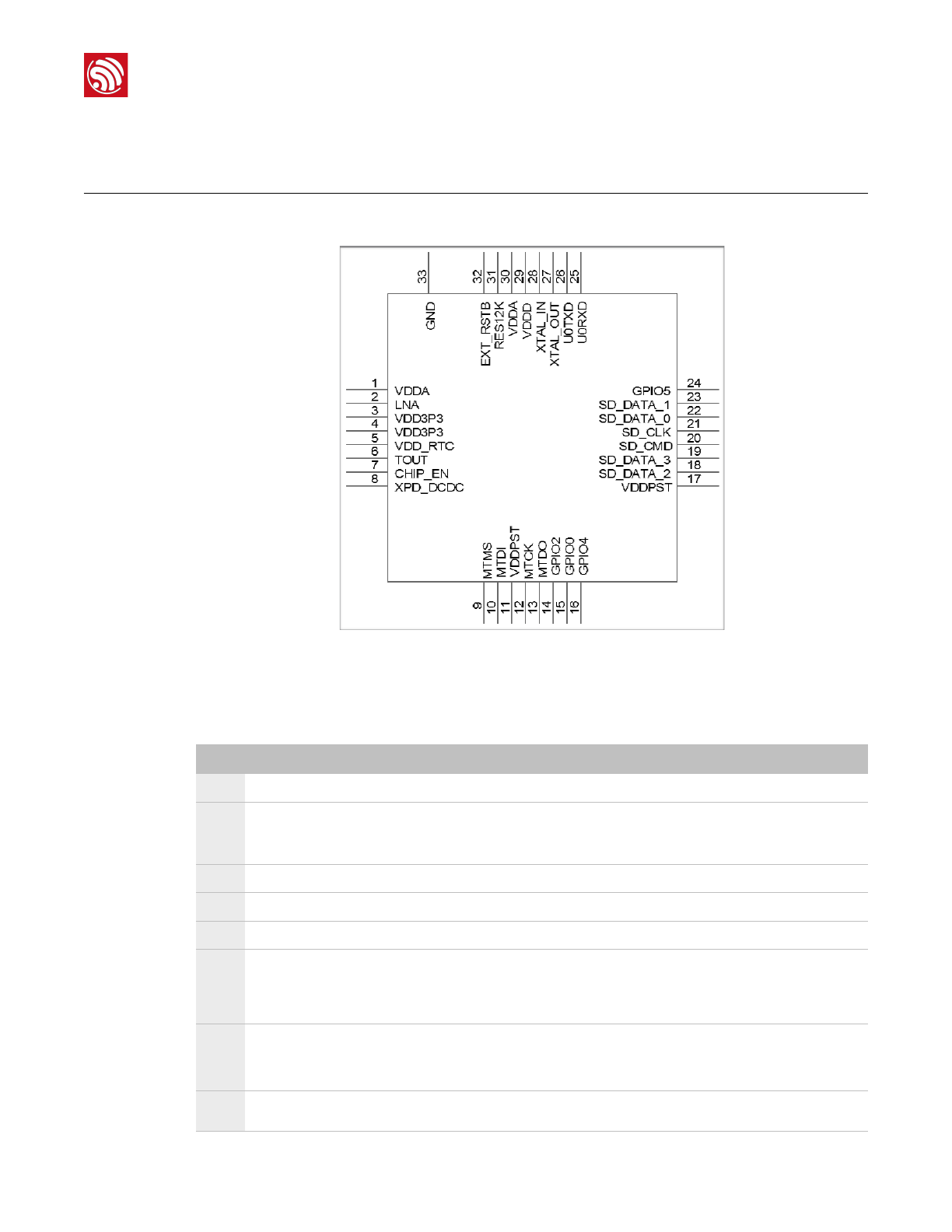
Figure 2-1 shows the pin layout for 32-pin QFN package.
!
Figure 2-1. Pin Layout
Table 2-1 lists the definitions and functions of each pin.
Table 2-1. ESP8266EX Pin Definitions
Pin
Name
Type
Function
1
VDDA
P
Analog Power 2.5V ~ 3.6V
2
LNA
I/O
RF antenna interface
Chip output impedance=39+j6 Ω. It is suggested to retain the
π-type matching network to match the antenna.
3
VDD3P3
P
Amplifier Power 2.5V ~ 3.6V
4
VDD3P3
P
Amplifier Power 2.5V ~ 3.6V
5
VDD_RTC
P
NC (1.1V)
6
TOUT
I
ADC pin. It can be used to test the power-supply voltage of
VDD3P3 (Pin3 and Pin4) and the input power voltage of TOUT
(Pin 6). However, these two functions cannot be used
simultaneously.
7
CHIP_PU
I
Chip Enable
High: On, chip works properly
Low: Off, small current consumed
8
XPD_DCDC
I/O
Deep-sleep wakeup (need to be connected to EXT_RSTB);
GPIO16
Espressif
% /%5 25
2017.04