
Data Sheet
%
3. Functional Description
3. Functional Description
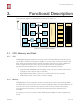
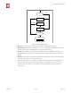
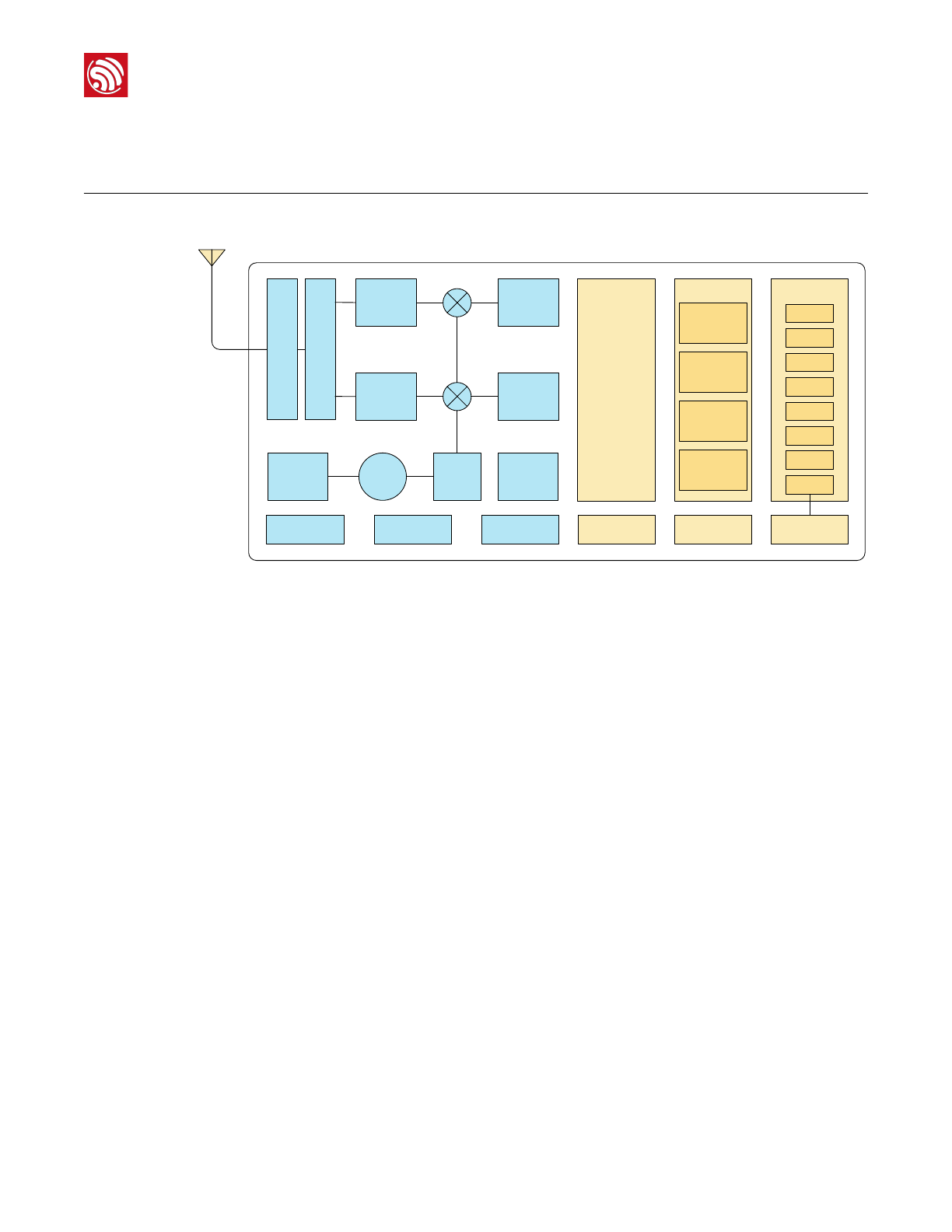
The functional diagram of ESP8266EX is shown as in Figure 3-1.
%
Figure 3-1. Functional Block Diagram
3.1. CPU, Memory, and Flash
3.1.1. CPU
ESP8266EX integrates Tensilica L106 32-bit micro controller (MCU) and ultra-low-power
16-bit RSIC. The CPU clock speed is 80 MHz. It can also reach a maximum value of 160
MHz. Real Time Operation System (RTOS) is enabled. Currently, only 20% of MIPS has
been occupied by the Wi-Fi stack, the rest can all be used for user application
programming and development. The CPU includes the interfaces as below.
• Programmable RAM/ROM interfaces (iBus), which can be connected with memory
controller, and can also be used to visit flash.
• Data RAM interface (dBus), which can connected with memory controller.
• AHB interface which can be used to visit the register.
3.1.2. Memory
ESP8266EX Wi-Fi SoC integrates memory controller and memory units including SRAM
and ROM. MCU can access the memory units through iBus, dBus, and AHB interfaces. All
memory units can be accessed upon request, while a memory arbiter will decide the
running sequence according to the time when these requests are received by the
processor.
According to our current version of SDK, SRAM space available to users is assigned as
below.
RF balun
Switch
RF
receive
RF
transmit
Analog
receive
Analog
transmit
PLL VCO 1/2 PLL
Digital baseband
MAC Interface
PMU Crystal Bias circuits SRAM PMU
SDIO
I2C
PWM
ADC
SPI
UART
GPIO
I2S
Flash
Registers
CPU
Sequencers
Accelerator
Espressif
% /%7 25
2017.04